- Electric and Telecom Plans Free
- Fire and Emergency Plans Free
- Floor Plans Free
- Plant Layout Plans Free
- School and Training Plans Free
- Seating Plans Free
- Security and Access Plans Free
- Site Plans Free
- Sport Field Plans Free
- Business Process Diagrams Free
- Business Process Mapping Free
- Classic Business Process Modeling Free
- Cross-Functional Flowcharts Free
- Event-driven Process Chain Diagrams Free
- IDEF Business Process Diagrams Free
- Logistics Flow Charts Free
- Workflow Diagrams Free
- ConceptDraw Dashboard for Facebook Free
- Mind Map Exchange Free
- MindTweet Free
- Note Exchange Free
- Project Exchange Free
- Social Media Response Free
- Active Directory Diagrams Free
- AWS Architecture Diagrams Free
- Azure Architecture Free
- Cisco Network Diagrams Free
- Cisco Networking Free
- Cloud Computing Diagrams Free
- Computer Network Diagrams Free
- Google Cloud Platform Free
- Interactive Voice Response Diagrams Free
- Network Layout Floor Plans Free
- Network Security Diagrams Free
- Rack Diagrams Free
- Telecommunication Network Diagrams Free
- Vehicular Networking Free
- Wireless Networks Free
- Comparison Dashboard Free
- Composition Dashboard Free
- Correlation Dashboard Free
- Frequency Distribution Dashboard Free
- Meter Dashboard Free
- Spatial Dashboard Free
- Status Dashboard Free
- Time Series Dashboard Free
- Basic Circle-Spoke Diagrams Free
- Basic Circular Arrows Diagrams Free
- Basic Venn Diagrams Free
- Block Diagrams Free
- Concept Maps Free
- Family Tree Free
- Flowcharts Free
- Basic Area Charts Free
- Basic Bar Graphs Free
- Basic Divided Bar Diagrams Free
- Basic Histograms Free
- Basic Line Graphs Free
- Basic Picture Graphs Free
- Basic Pie Charts Free
- Basic Scatter Diagrams Free
- Aerospace and Transport Free
- Artwork Free
- Audio, Video, Media Free
- Business and Finance Free
- Computers and Communications Free
- Holiday Free
- Manufacturing and Maintenance Free
- Nature Free
- People Free
- Presentation Clipart Free
- Safety and Security Free
- Analog Electronics Free
- Audio and Video Connectors Free
- Basic Circuit Diagrams Free
- Chemical and Process Engineering Free
- Digital Electronics Free
- Electrical Engineering Free
- Electron Tube Circuits Free
- Electronic Block Diagrams Free
- Fault Tree Analysis Diagrams Free
- GHS Hazard Pictograms Free
- Home Automation and Wiring Free
- Mechanical Engineering Free
- One-line Diagrams Free
- Power Сircuits Free
- Specification and Description Language (SDL) Free
- Telecom and AV Circuits Free
- Transport Hazard Pictograms Free
- Data-driven Infographics Free
- Pictorial Infographics Free
- Spatial Infographics Free
- Typography Infographics Free
- Calendars Free
- Decision Making Free
- Enterprise Architecture Diagrams Free
- Fishbone Diagrams Free
- Organizational Charts Free
- Plan-Do-Check-Act (PDCA) Free
- Seven Management and Planning Tools Free
- SWOT and TOWS Matrix Diagrams Free
- Timeline Diagrams Free
- Australia Map Free
- Continent Maps Free
- Directional Maps Free
- Germany Map Free
- Metro Map Free
- UK Map Free
- USA Maps Free
- Customer Journey Mapping Free
- Marketing Diagrams Free
- Matrices Free
- Pyramid Diagrams Free
- Sales Dashboard Free
- Sales Flowcharts Free
- Target and Circular Diagrams Free
- Cash Flow Reports Free
- Current Activities Reports Free
- Custom Excel Report Free
- Knowledge Reports Free
- MINDMAP Reports Free
- Overview Reports Free
- PM Agile Free
- PM Dashboards Free
- PM Docs Free
- PM Easy Free
- PM Meetings Free
- PM Planning Free
- PM Presentations Free
- PM Response Free
- Resource Usage Reports Free
- Visual Reports Free
- House of Quality Free
- Quality Mind Map Free
- Total Quality Management TQM Diagrams Free
- Value Stream Mapping Free
- Astronomy Free
- Biology Free
- Chemistry Free
- Language Learning Free
- Mathematics Free
- Physics Free
- Piano Sheet Music Free
- Android User Interface Free
- Class Hierarchy Tree Free
- Data Flow Diagrams (DFD) Free
- DOM Tree Free
- Entity-Relationship Diagram (ERD) Free
- EXPRESS-G data Modeling Diagram Free
- IDEF0 Diagrams Free
- iPhone User Interface Free
- Jackson Structured Programming (JSP) Diagrams Free
- macOS User Interface Free
- Object-Role Modeling (ORM) Diagrams Free
- Rapid UML Free
- SYSML Free
- Website Wireframe Free
- Windows 10 User Interface Free
Analog Electronics
The electronics technologies, electrical circuits, electronic components and electronic devices are widespread worldwide. They use digital and analog technologies and their combinations. But mainly our world is analog and all the waves in the electromagnetic spectrum are analog as well.
The analog electronics and circuits work with continuously variable analog signals. The signals are passed among devices and transmit information in the form of audio, video or encoded data. The analog circuits are durable and widely used in radio and audio equipment. The AC and DC systems, mechanical, pneumatic, hydraulic systems also require analog components and may use analog signals. At the same time, both simple and complex analog circuits are built for different purposes. Most analog circuits are difficult to design, require high precision, and are very sensitive to noise.
Sometimes analog signals are an intermediate step between real-world information and digital ones, where sensors create analog signals from real-world information and then convert them to digital. Analog signals take a value from a given range and also use the attributes of the environment. Wired or airborne transmission using RF waves, amplification, filtering, clipping and other operations are performed on analog signals.
Often analog systems include the noise that causes signal degradation. This noise is formed by random disturbances caused by the random thermal vibrations of atomic particles or crosstalk from other signals. Sometimes it is caused by random variations in result of copy the signals transmitted over long distances. The effect of noise on the analog circuit directly depends on its level. The greater level of noise is, the more distortions the analog signal has. The filtering with an analog unit is used to remove the noise from a signal.
Analog circuits consist of active and passive electrical components. Active components such as transistors and op amps are powered by a voltage source, consume electricity, and can control and modify electrical signals. Passive components do not consume electricity to operate. These are resistors, capacitors, inductors, diodes and other electronic components.
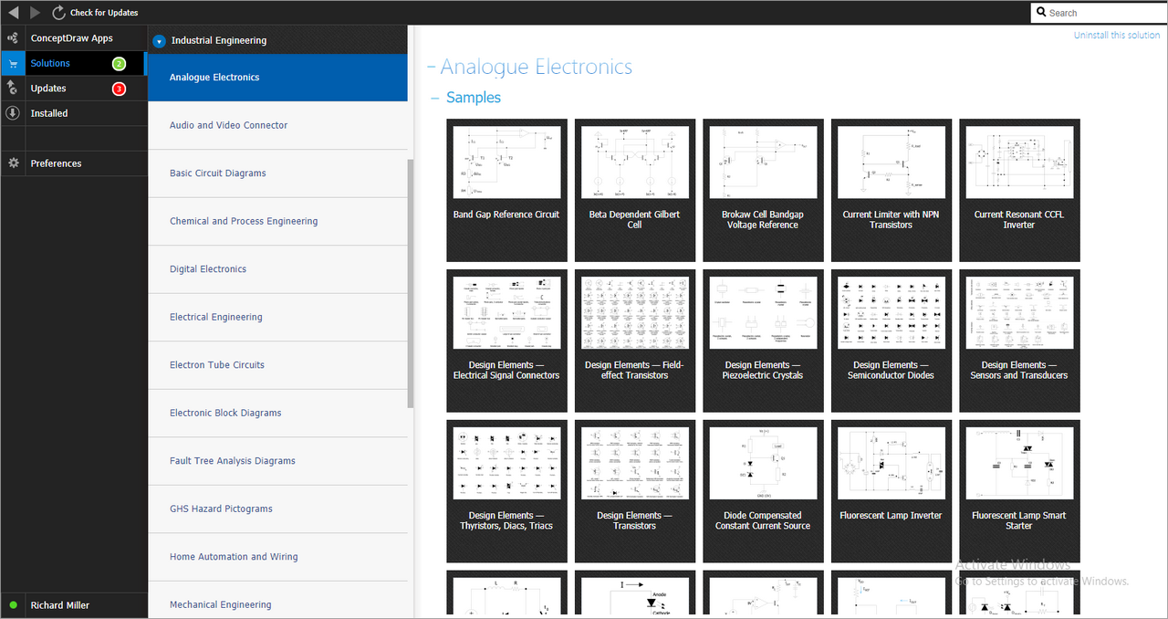
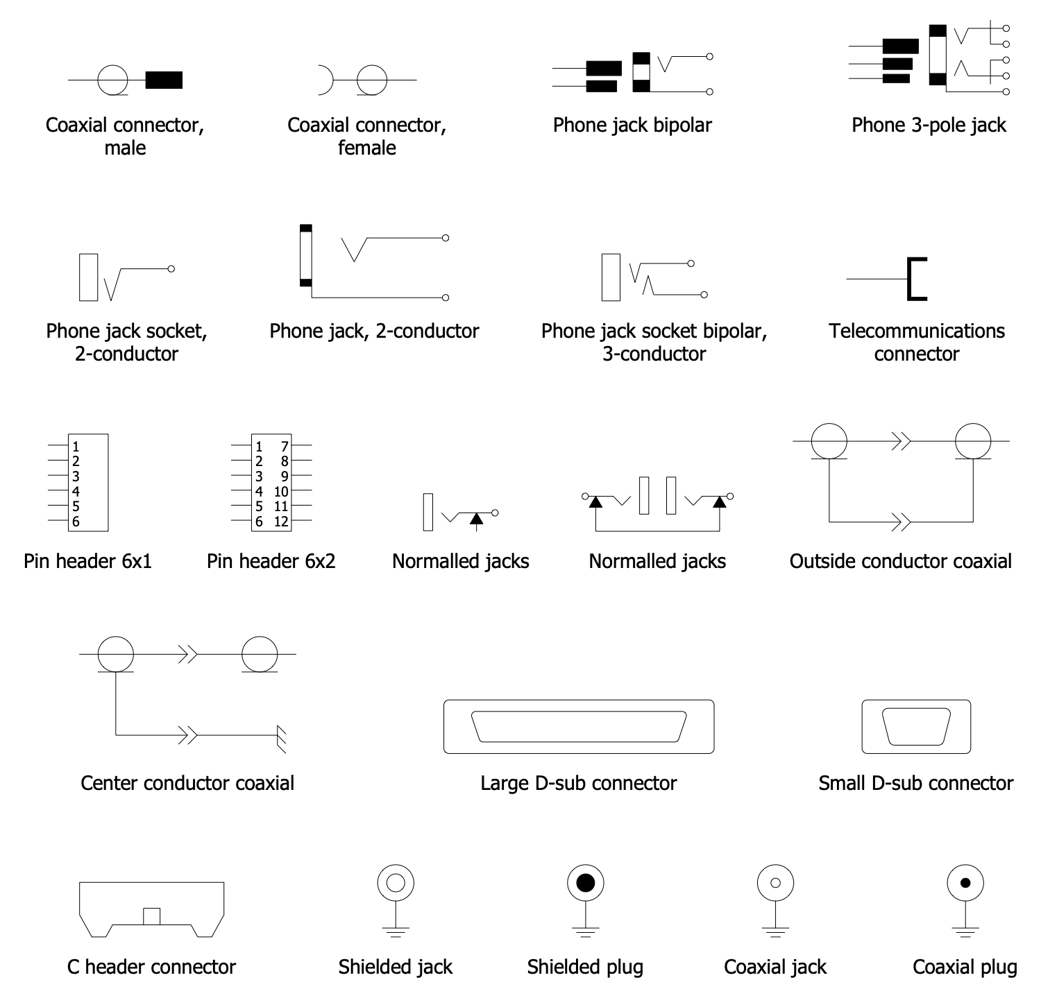
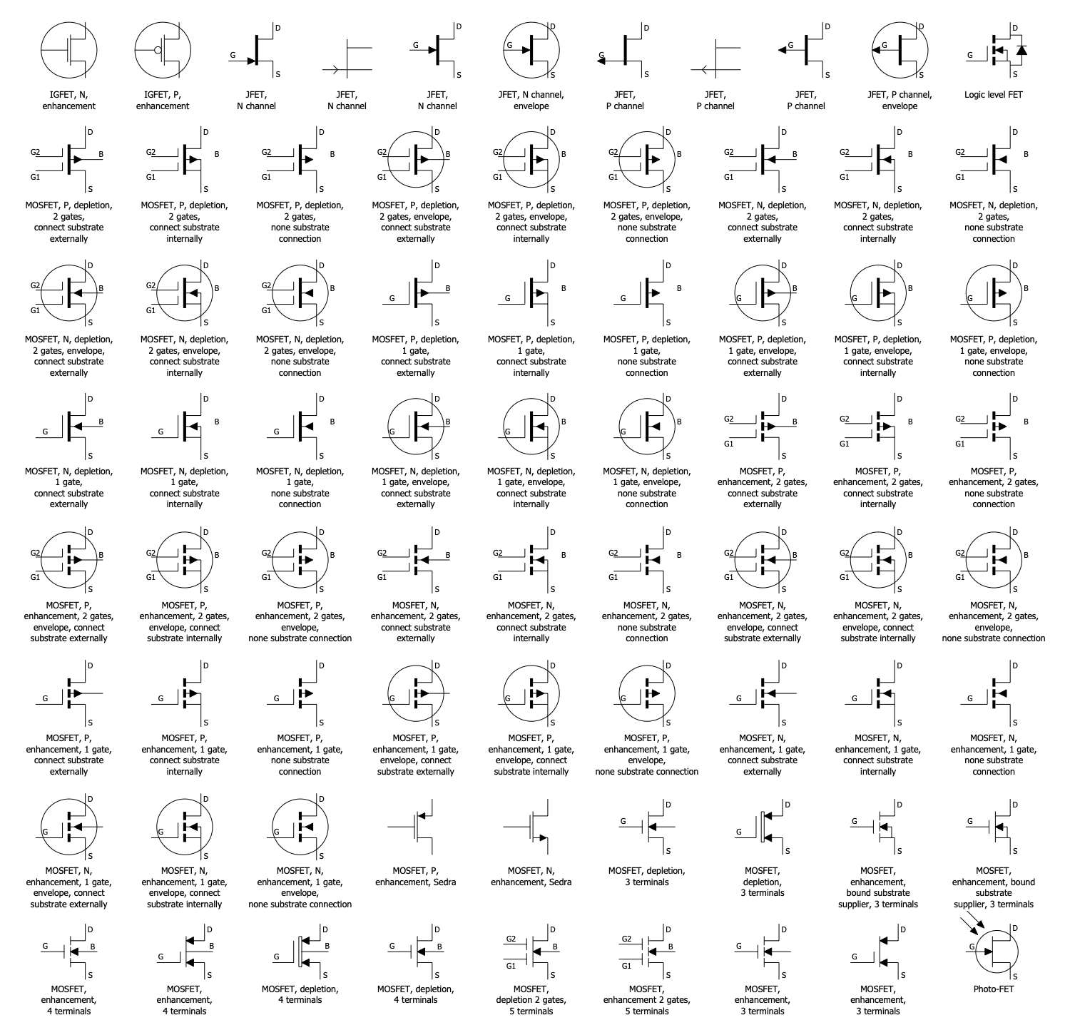
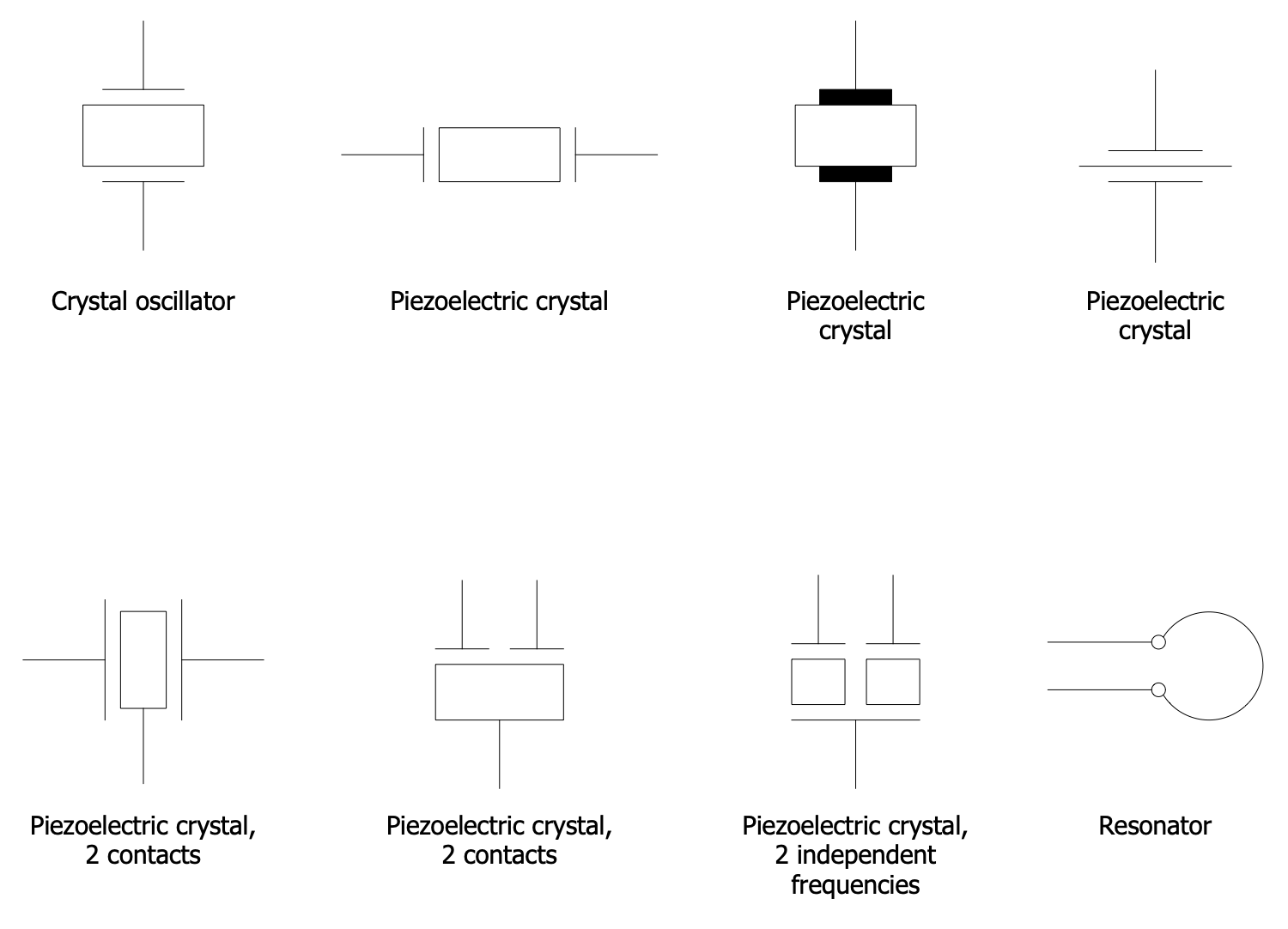
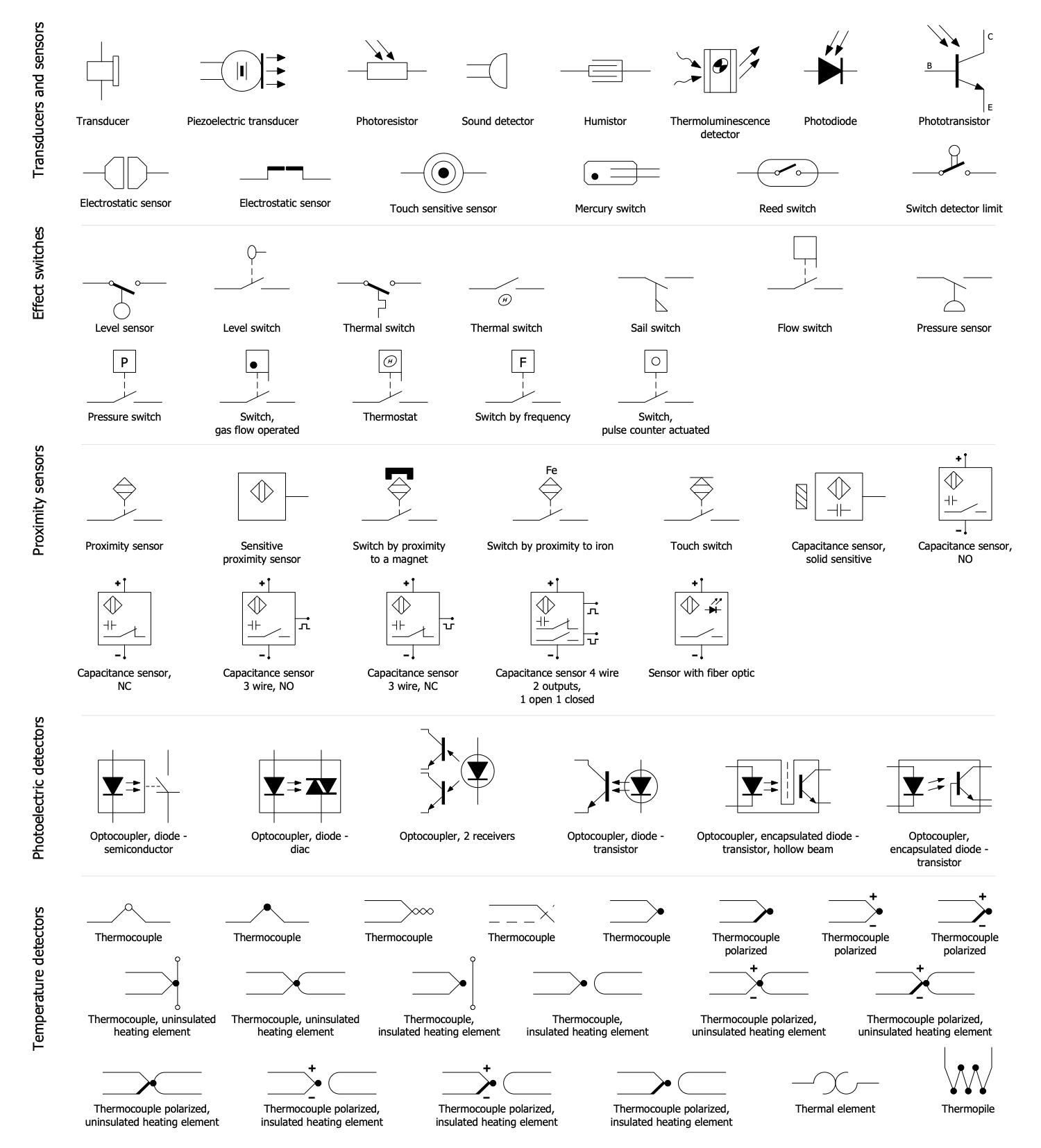
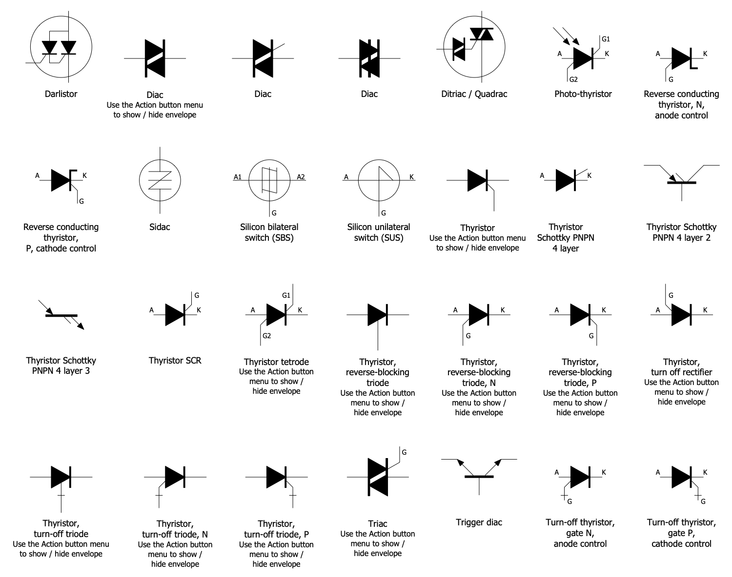
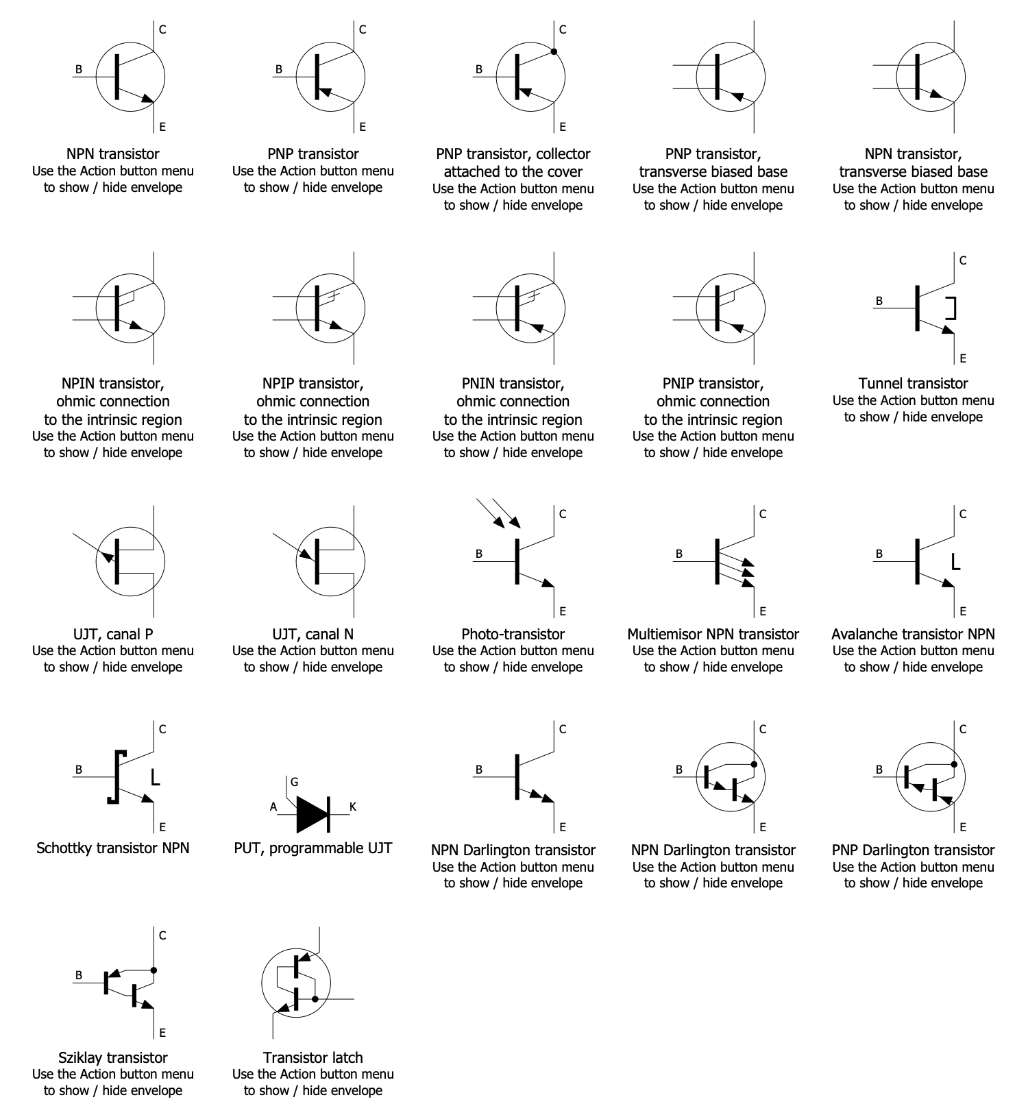
The Analog Electronics solution extends ConceptDraw DIAGRAM with a set of samples and a collection of predesigned special objects and analog electronics symbols common for designing analog circuits. They include electrical signal connectors, transistors, semiconductors, diodes, sensors, transducers, thyristors, crystals, diacs, etc. This solution is incredibly helpful to construct analog electronic circuits, electronic engineering designs, electrical engineering diagrams and schematics of different complexity. It is incredibly useful for electrical engineers, electronic designers and developers, electricians, mechanics, and more electronics-related specialists.
-
What I need to get started -
Solution Requirements - This solution requires the following products to be installed:
ConceptDraw DIAGRAM v18 - This solution requires the following products to be installed:
-
Support for this Solution -
Helpdesk
Design Elements — Electrical Signal Connectors
Design Elements — Field Effect Transistors
Design Elements — Piezoelectric Crystals
Design Elements — Semiconductor Diodes
Design Elements — Sensors and Transducers
Design Elements — Thyristors Diacs Triacs
Design Elements — Transistors
Related News:
Examples
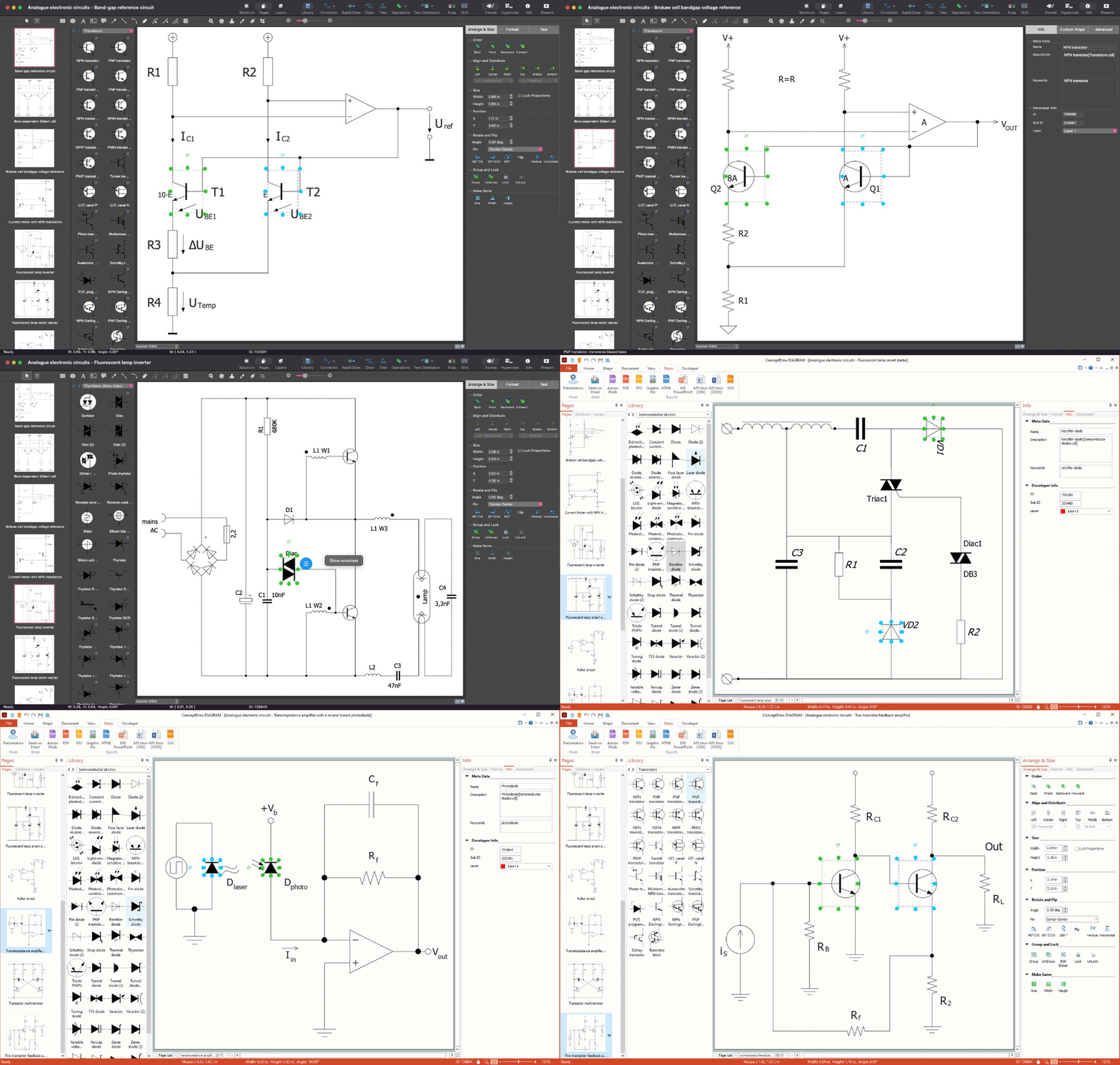
There are a few samples that you see on this page which were created in the ConceptDraw DIAGRAM application by using the Analogue Electronics solution. Some of the solution's capabilities as well as the professional results which you can achieve are all demonstrated here on this page.
All source documents are vector graphic documents which are always available for modifying, reviewing and/or converting to many different formats, such as MS PowerPoint, PDF file, MS Visio, and many other graphic ones from the ConceptDraw Solution Park or ConceptDraw STORE. The Analogue Electronics solutions are available to all ConceptDraw DIAGRAM users to install and use it for working in diagramming and drawing.
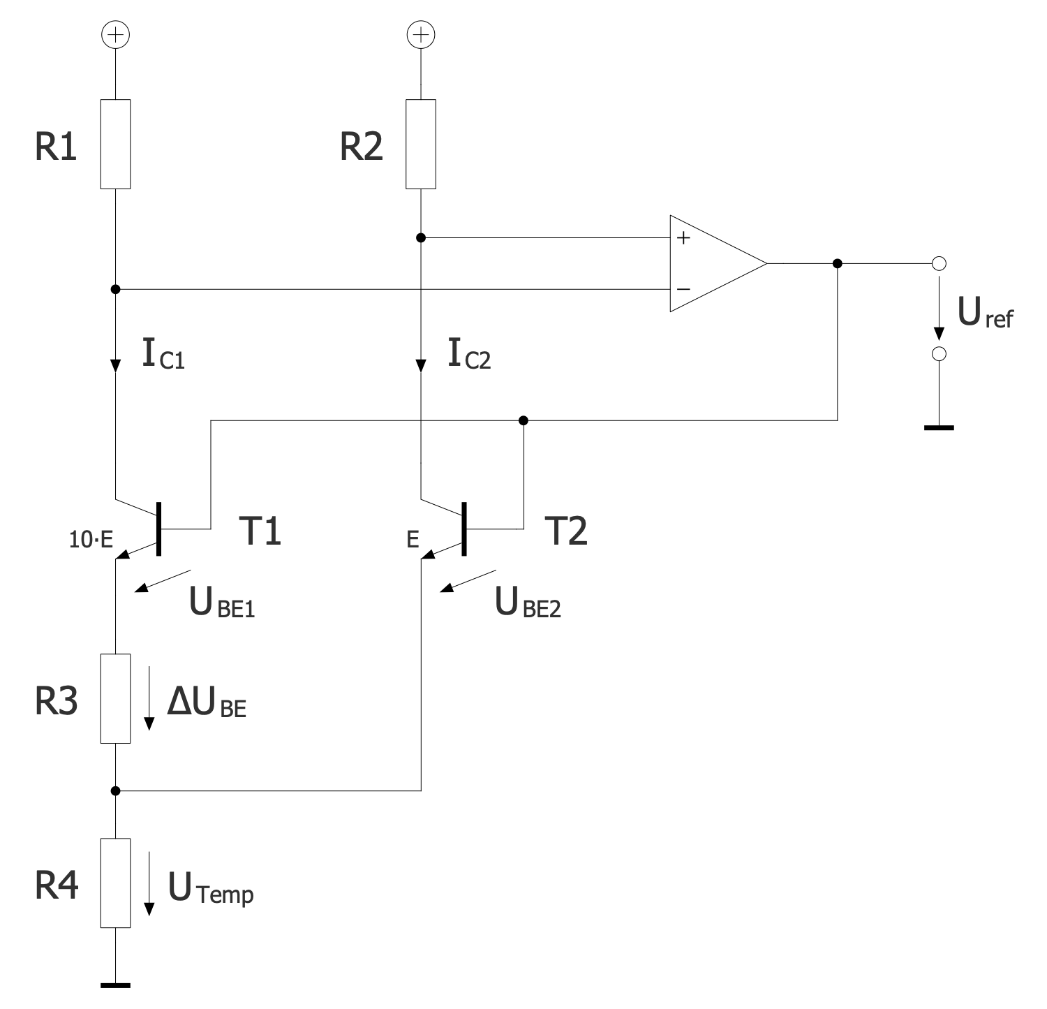
Example 1: Band Gap Reference Circuit
This diagram was created in ConceptDraw DIAGRAM using a combination of libraries from the Analog Electronics Solution. An experienced user spent 10 minutes creating this sample.
This sample of analog electronics shows the bandgap voltage reference circuit invented by David Hilbiber in 1964. This is a circuit that produces a constant voltage regardless of many factors, including fluctuations in the power supply, temperature changes, circuit load from the device, etc. The band gap reference is a temperature-independent voltage reference circuit. The bandgap reference includes BJT devices and resistors. The typical output voltage is about 1.25V. The current is generated due to the voltage difference between the two p-n junctions and is proportional to the absolute temperature (PTAT) in the resistor. For example, diodes operating at different current densities can generate current. This current is then used to create voltage in a second resistor, then in a third, or added to the voltage across one of the junctions. The band gap reference is often used in integrated circuits and voltage regulators.
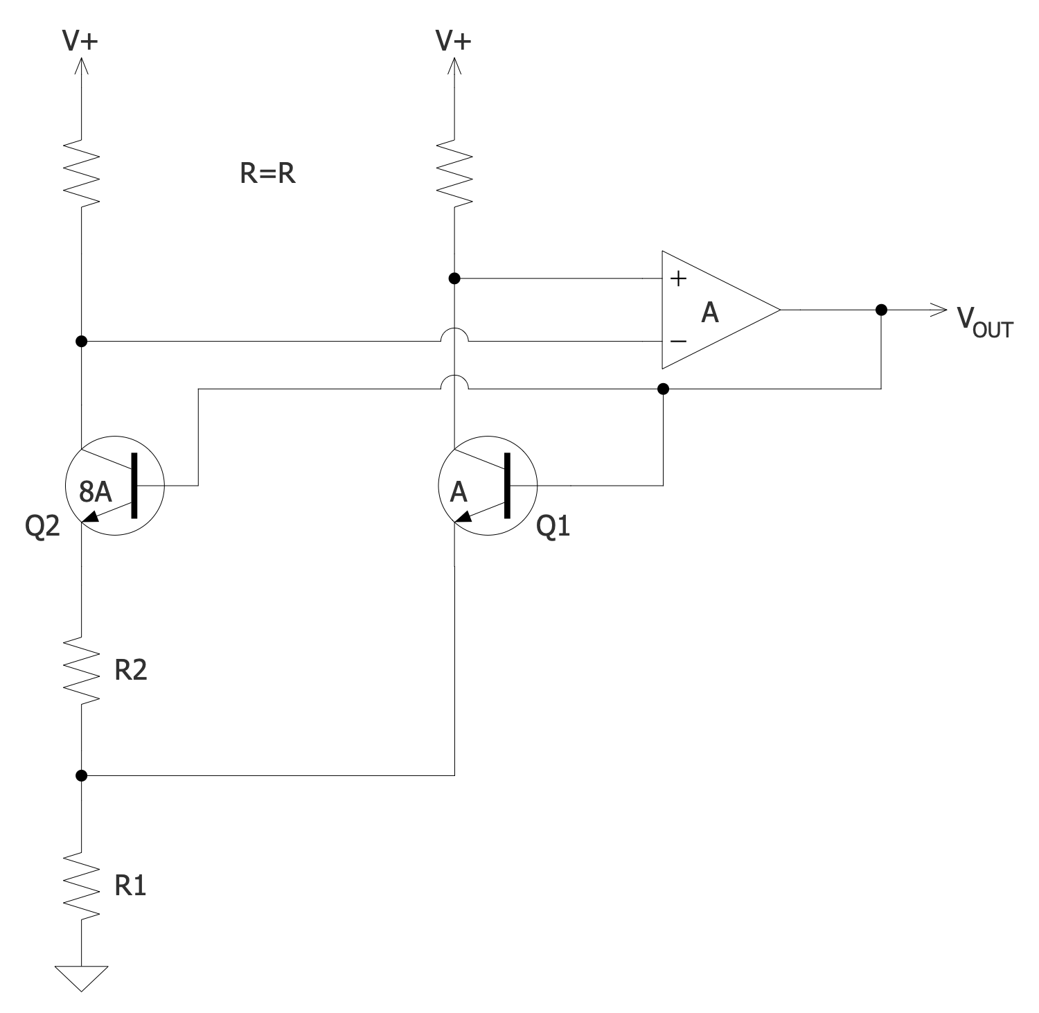
Example 2: Brokaw Cell Bandgap Voltage Reference
This diagram was created in ConceptDraw DIAGRAM using a combination of libraries from the Analog Electronics Solution. An experienced user spent 10 minutes creating this sample.
This sample shows a theoretical circuit of the Brokaw bandgap voltage reference, named after its inventor Paul Brokaw. It is used in integrated circuits with an output voltage of 1.25 V and low temperature dependence. This circuit maintains two internal voltage sources — positive and negative temperature coefficients. By summing these opposite coefficients, the temperature dependence can be cancelled. In this case, any of these two internal sources can be used as temperature sensors. Negative feedback is used by the circuit to supply DC current through two bipolar transistors with different emitter areas. A transistor with a larger emitter area requires less base-emitter voltage for the same current. The op-amp provides the same voltage for both the inverting and non-inverting input. The currents in the collector resistors are the same, the collector currents of Q1 and Q2 are also the same. If Q2 has an emitter area larger than Q1, its base-emitter voltage will be lower than Q1's.
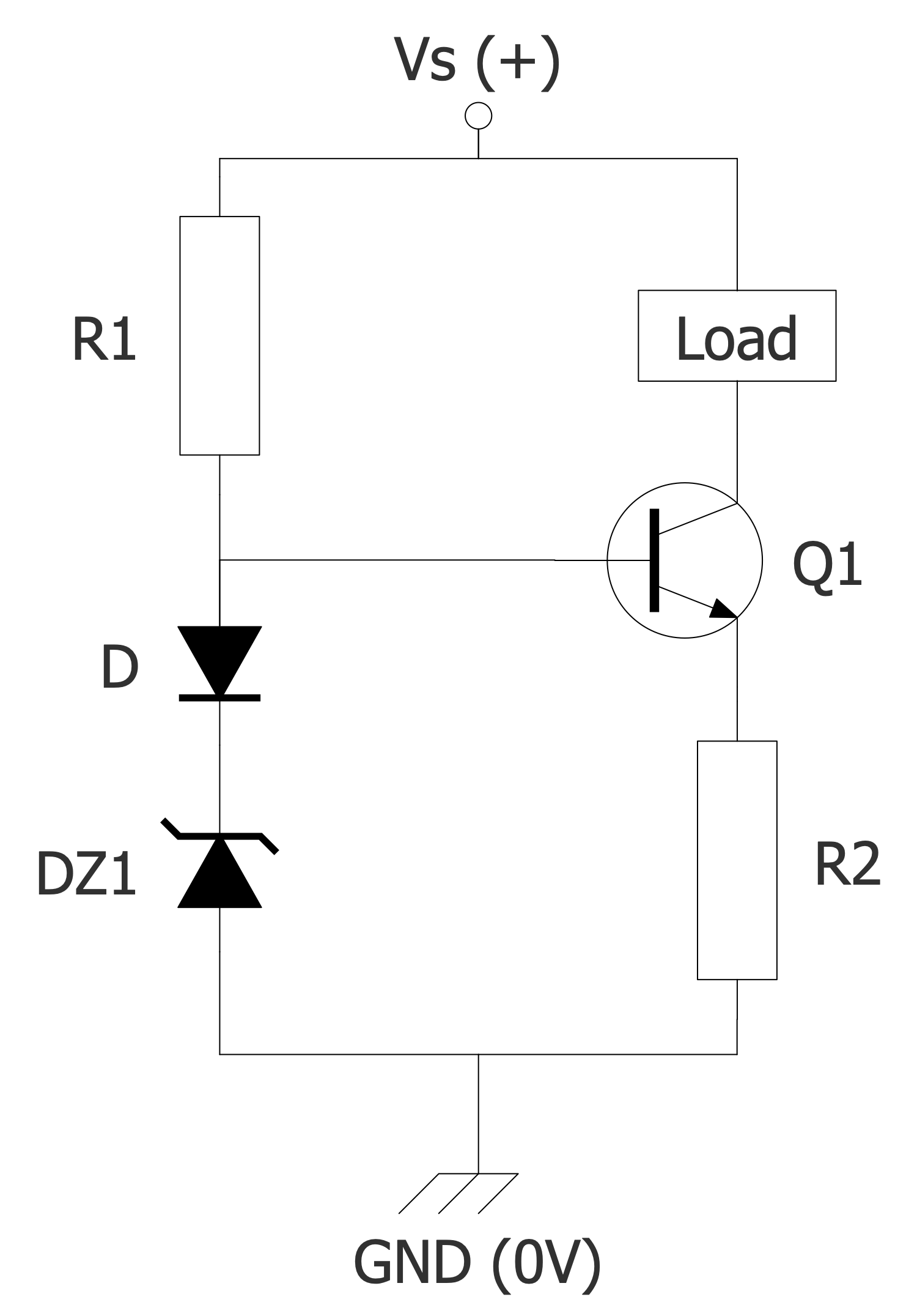
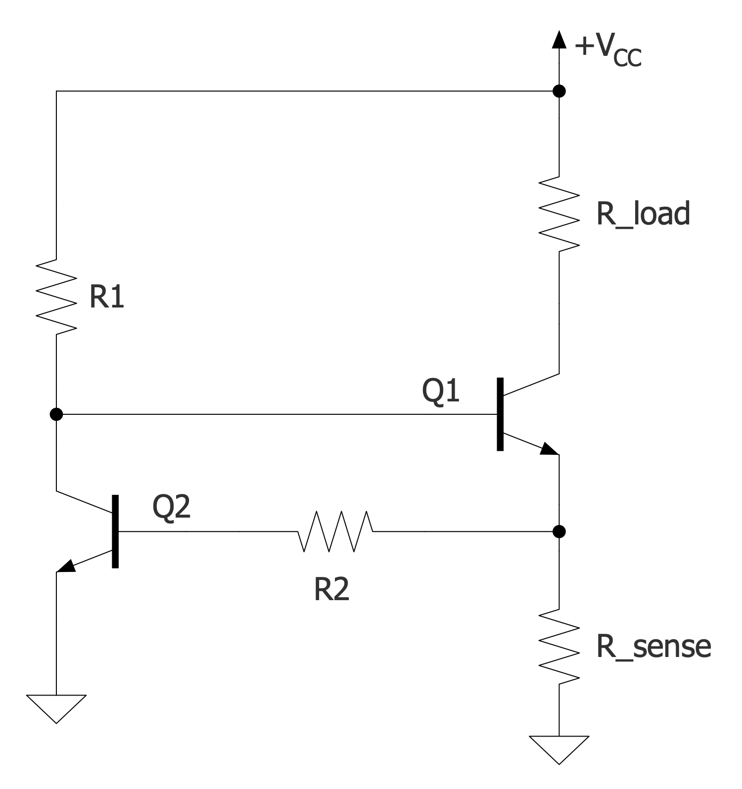
Example 3: Current Limiter with NPN Transistors
This diagram was created in ConceptDraw DIAGRAM using a combination of libraries from the Analog Electronics Solution. An experienced user spent 10 minutes creating this sample.
This electronic engineering sample shows the way of a current limiting circuit by a current limiter with NPN transistors. The actions on current limiting provide protection of the circuit from the harmful effects of a short circuit or overload. A simple protection mechanism used in regulated DC supplies and class-AB power amplifiers is shown. Q1 is the output transistor and Q2 is the protection transistor. R1 allows Q1 to turn on, then it passes voltage and current to the load. R2 is an optional component, it protects Q2 in the event of a short-circuited load. R_sense is the load current sensing device. When it exceeds the design limit, Q2 turns on, Q1 turns off and limits the load current. This schematic has a practical application as a current source for high-power LEDs. The power dissipation is realized until the overload exists. The output voltage is decreased to a value depending on the load resistance and current limit. Under overload, the output voltage falls, the difference increases and leads to increasing dissipation.
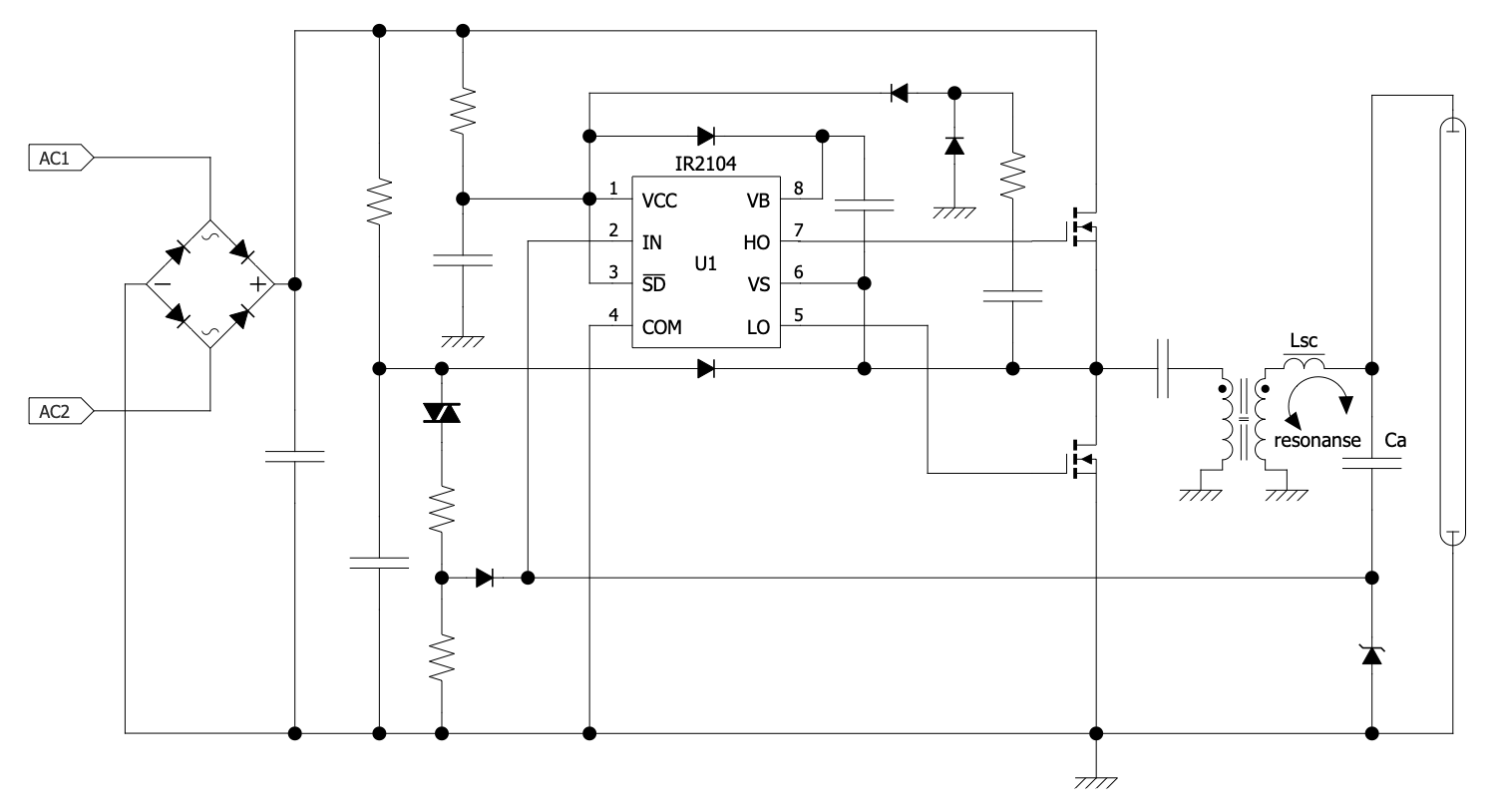
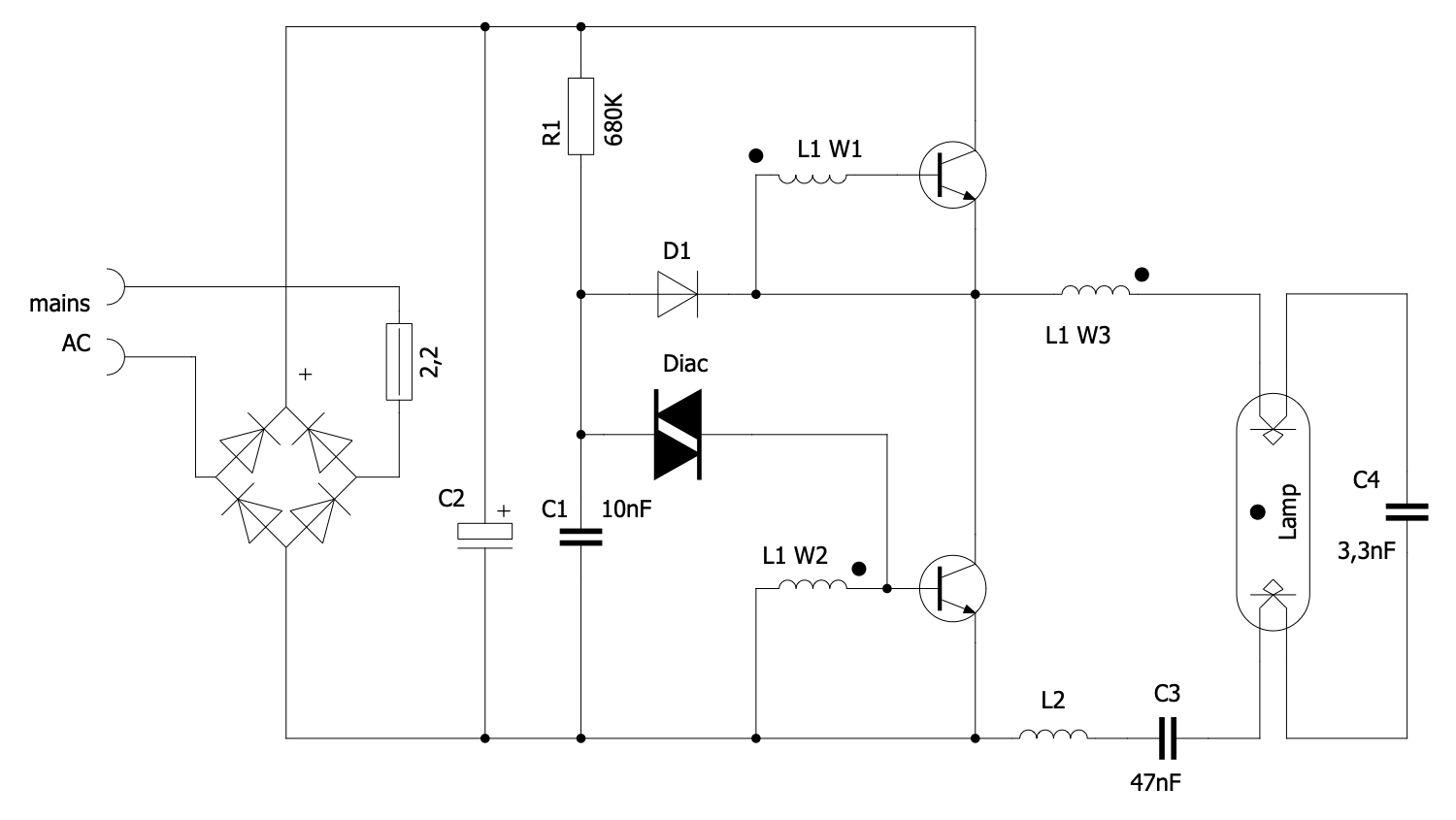
Example 4: Fluorescent Lamp Inverter
This diagram was created in ConceptDraw DIAGRAM using a combination of libraries from the Analog Electronics Solution. An experienced user spent 15 minutes creating this sample.
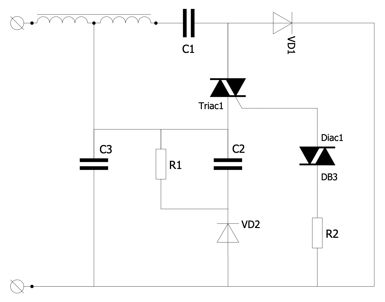
This sample shows a fluorescent lamp inverter circuit. This is a low pressure mercury gas discharge lamp. This lamp uses fluorescence to produce visible light. The phosphor coating inside the lamp glows as a result of exciting an electric current in the gas, evaporating mercury, generating short-wavelength ultraviolet light. Fluorescent lamps convert electrical energy into usable light and are more efficient than incandescent lamps. The luminous efficiency of fluorescent lamps is several times higher than that of incandescent lamps. Fluorescent lamps are energy efficient but more expensive. Additional ballast is required to regulate the current through the lamp. Electronic ballasts include transistors used to convert power frequency AC power to high frequency AC power, a simple oscillator, and an LC series resonant circuit. However, the mercury content makes fluorescent lamps hazardous waste, so they must be separated from general waste and recycled.
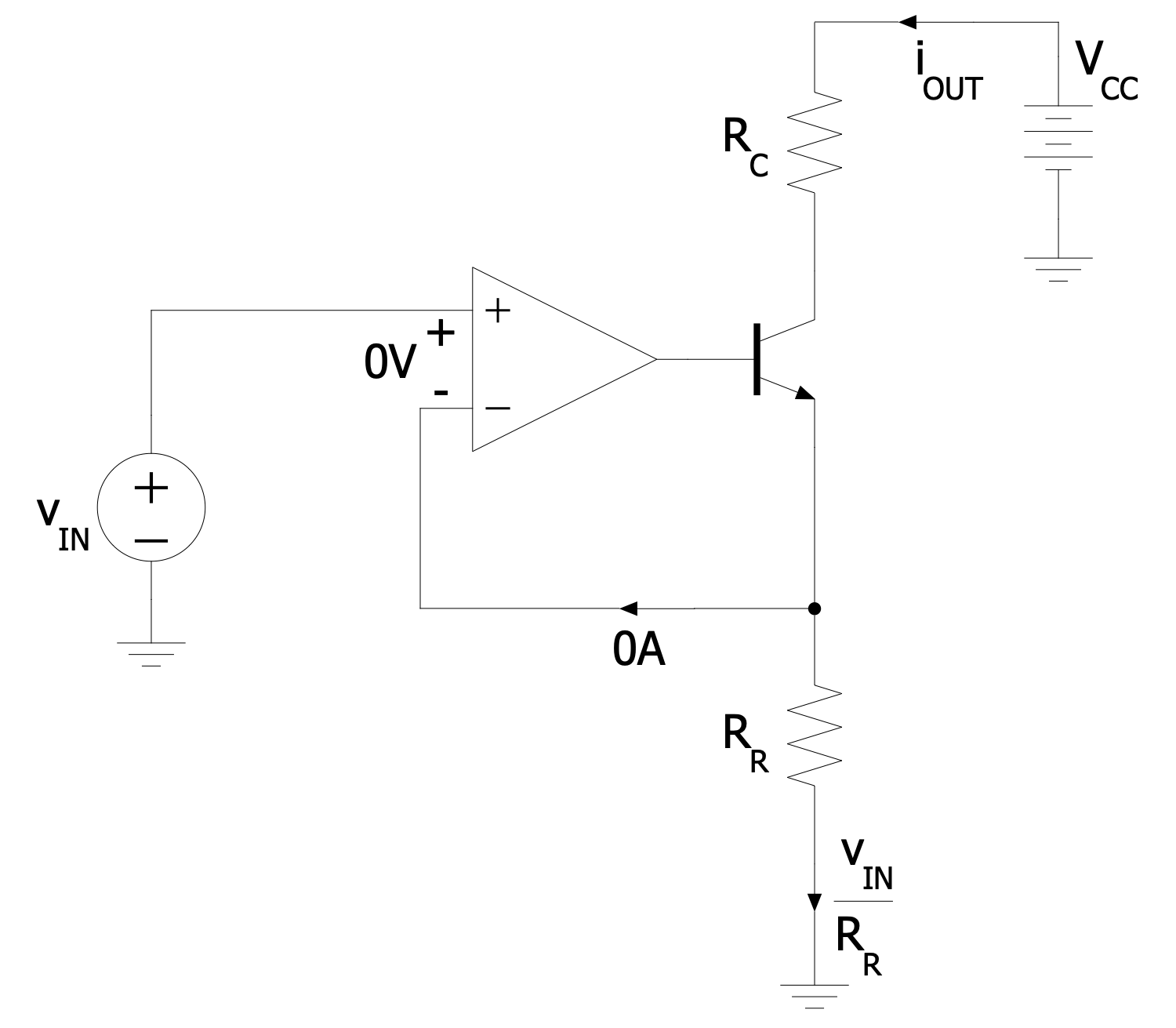
Example 5: Nullor Circuit
This diagram was created in ConceptDraw DIAGRAM using a combination of libraries from the Analog Electronics Solution. An experienced user spent 10 minutes creating this sample.
This sample shows the nullor, which is a theoretical two-port network and an ideal amplifier with infinite current, transconductance, voltage, and transimpedance gain. It includes a nullator at the input and a norator at the output. All transfer parameters of the nullor are equal to zero. Once included in a schema, nulllor affects its behavior and imposes mathematical restrictions on it. This example shows a voltage controlled current sink. The drain draws the same current Iout and is independent of the applied voltage Vcc at the output. The input voltage Vin sets the value of the current. The input current to nullor is zero. In turn, the voltage across the reference resistor RR is equal to the applied voltage Vin. Nullor provides any required current and does not depend on the voltage at its output. The output current depends on the user applied input voltage Vin and the reference resistor RR. The transistor included in the circuit provides a decrease in current in the PP, fed by the op-amp.
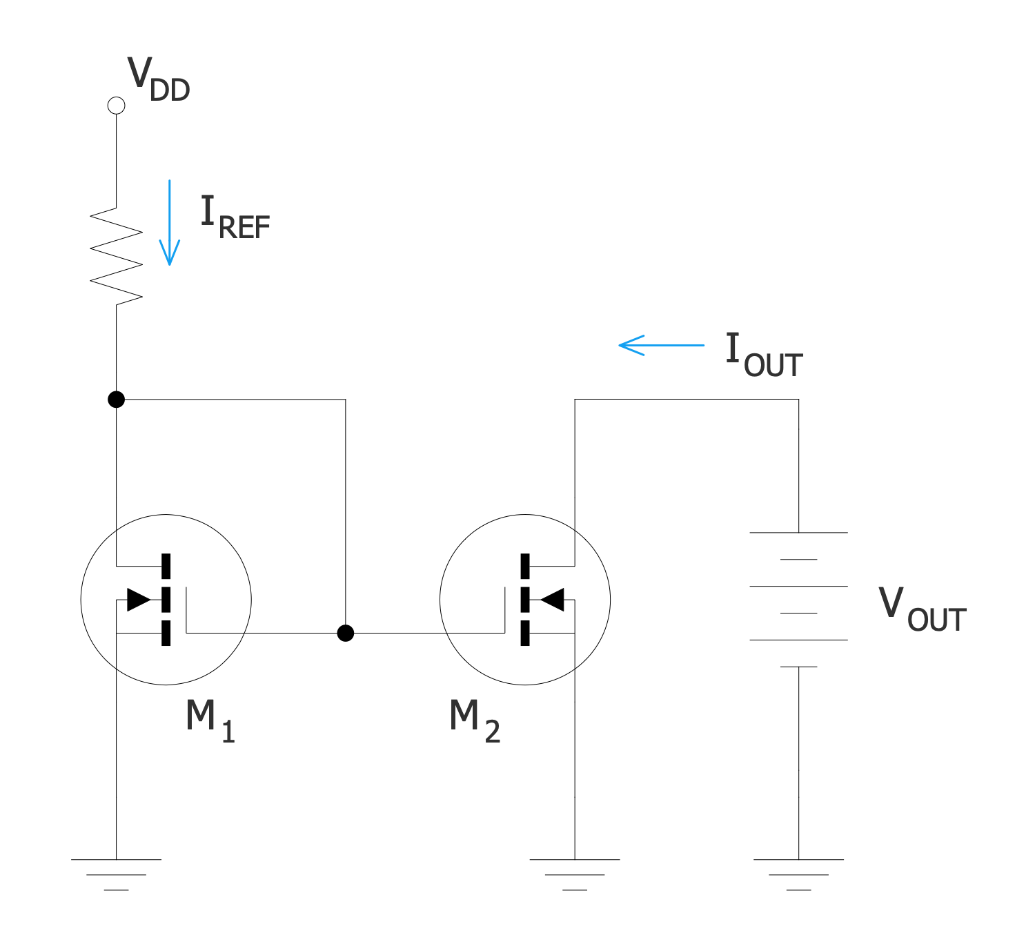
Example 6: Simple MOSFET Mirror
This diagram was created in ConceptDraw DIAGRAM using a combination of libraries from the Analog Electronics Solution. An experienced user spent 10 minutes creating this sample.
This electrical engineering sample shows the current mirror of a MOSFET. This circuit is designed to copy current through an active device while it is being driven by another active device in this circuit. In this case, the output current is kept constant regardless of the load. A current mirror is an ideal current inverting amplifier that reverses current direction. It allows you to apply bias currents and resistive loads in circuits that simulate a current source. Moreover, it may consist of a current-controlled current source. The current mirror is used in microcircuits. The current mirror MOSFET includes MOSFETs (M1 and M2) that operate in saturation or active mode and are used to set the reference current Iref. Vdd is the supply voltage, the output current Iout is directly related to Iref. MOSFET drain current depends on both the gate-to-source voltage and the drain-to-gate voltage. The reference current Iref is provided by a resistor, a current source with a set threshold, or a current source with auto-bias. This ensures constancy and independence from changes in supply voltage.
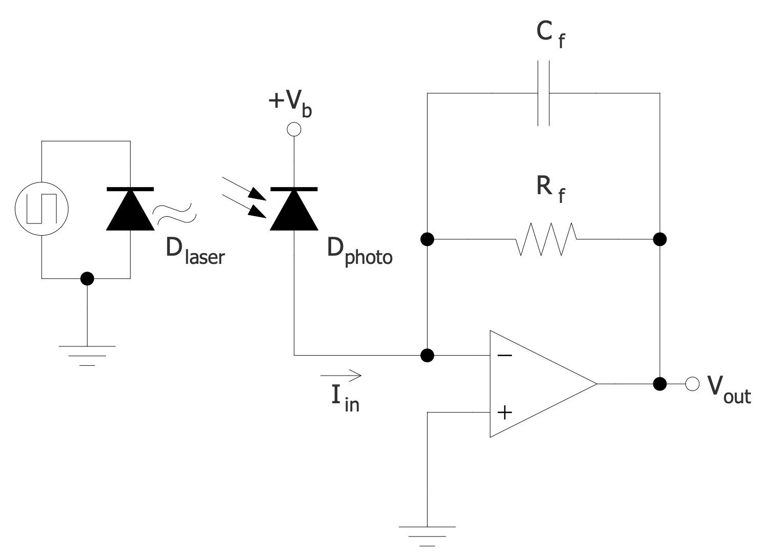
Example 7: Transimpedance Amplifier with a Reverse Biased Photodiode
This diagram was created in ConceptDraw DIAGRAM using a combination of libraries from the Analog Electronics Solution. An experienced user spent 10 minutes creating this sample.
This sample shows a transimpedance amplifier (TIA) with a reverse-based photodiode. TIA is a current to voltage converter. It allows you to amplify the output current of Geiger-Muller tubes, accelerometers, photodetectors, photomultipliers, etc. It includes one or more operational amplifiers. As a rule, transimpedance amplifiers are used with sensors that have a linear current characteristic. They provide a low resistance photodiode. In addition, TIAs isolate the photodiode from the output voltage of the operational amplifier. The proposed TIA includes a high resistance feedback resistor Rf. It sets the gain of the amplifier and is equal to -Rf due to the inverting configuration of the amplifier. Various configurations of transimpedance amplifiers are used. Each is suitable for a specific application, but they all require the sensor's low-level current to be converted to voltage. The photodiode is used as a current source, connected to ground and operates in photovoltaic mode without external bias. This provided a low photodiode voltage and a low impedance load.
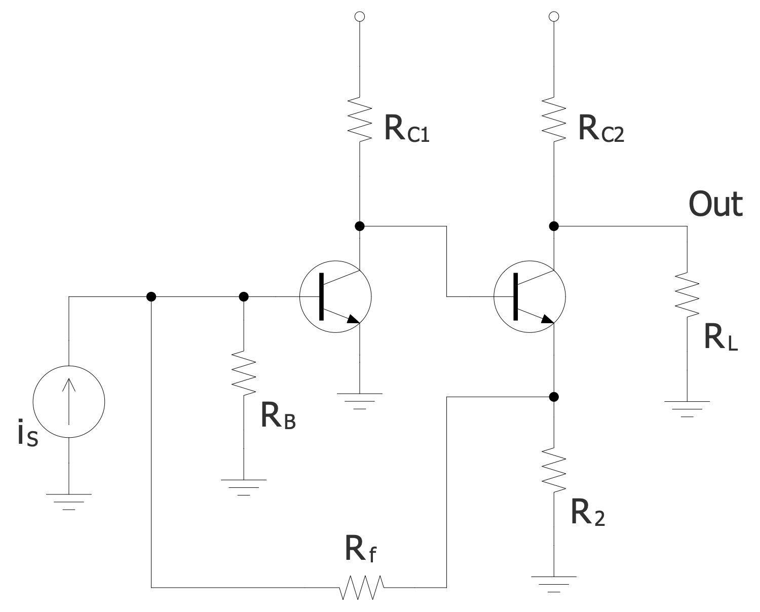
Example 8: Two Transistor Feedback Amplifier
This diagram was created in ConceptDraw DIAGRAM using a combination of libraries from the Analog Electronics Solution. An experienced user spent 10 minutes creating this sample.
This sample shows a two-transistor amplifier with a feedback resistor Rf also called a shunt-series feedback amplifier. Its circuit includes many resistors. Resistor R2 is in series with the output and measures the output current. Resistor Rf is connected in parallel with the input and subtracts the input current from it. The source impedance Rs is combined with the base resistor Rb. The amplifier uses current feedback. The output node is also shown in the diagram. This sample simplifies circuit analysis to calculate various electrical circuit indicators. You can calculate gain, amplifier input impedance from source, amplifier output impedance from load, and more. The pre-built vector objects included in the ConceptDraw Analog Electronics solution libraries make it ideal for designing any analog circuit in minutes.
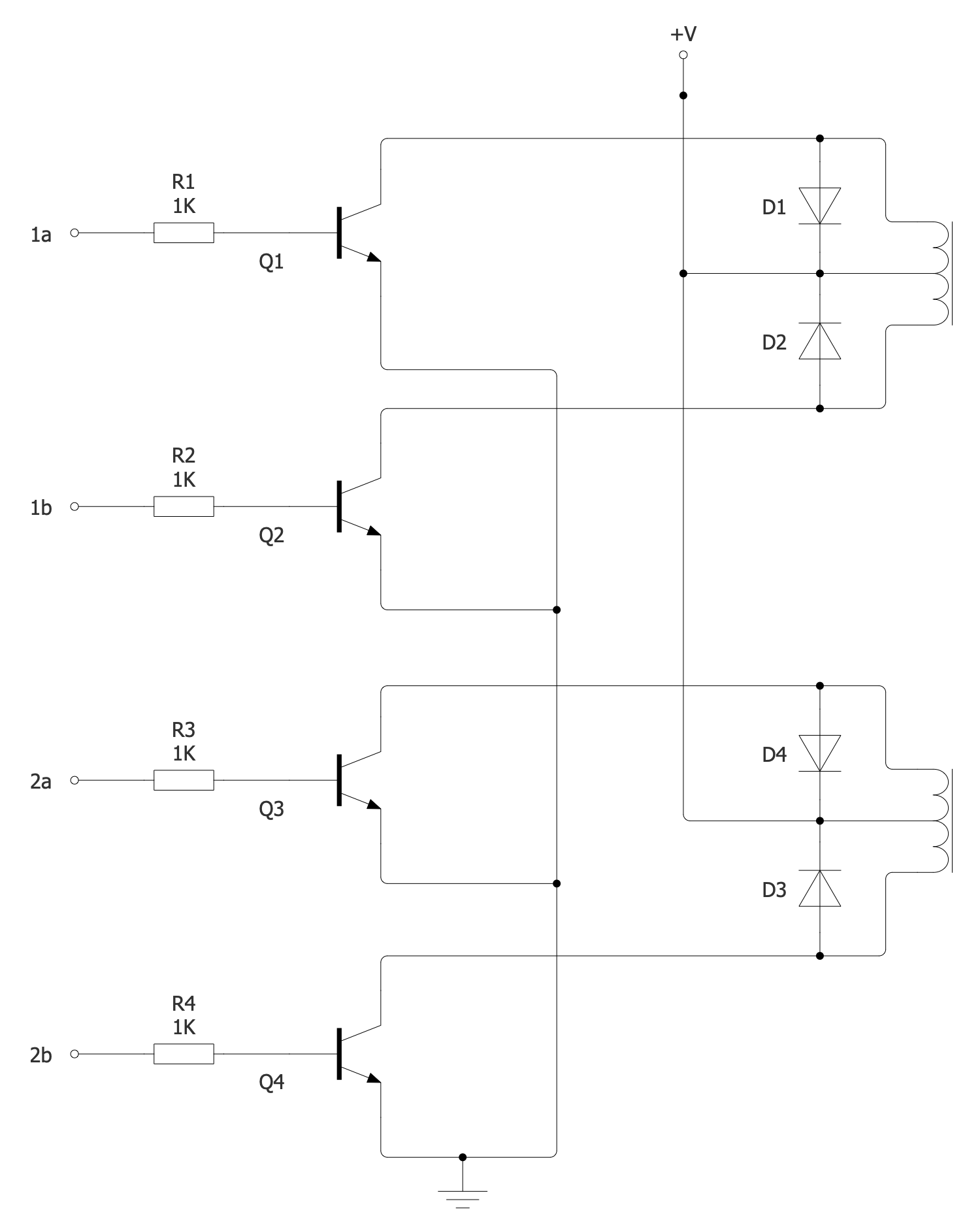
Example 9: Unipolar Stepper Motor Driver
This diagram was created in ConceptDraw DIAGRAM using a combination of libraries from the Analog Electronics Solution. An experienced user spent 15 minutes creating this sample.
This sample shows a unipolar stepper motor driver circuit. This is a device that rotates a shaft through a small predetermined angle, typically 1 to 5 degrees. Unipolar motors consist of a complex coil system and are easy to control. Each coil of a unipolar motor has three connections and includes a center tap. In total, unipolar motors have six leads (two groups of three) or five when connecting the middle leads. Physically, the wires are grouped in triplets and connected to a small printed circuit board. Unipolar motors do not need H-bridge drivers, and this is their key advantage. You just need to apply high voltage to one of the connectors to power the coil and turn off the opposite end. The windings in unipolar motors are bifilar, two coils are wound on top of each other, they connect the connectors "a" and "b" with the central tap. Voltage is applied to terminals 1a, 1b, 2a and 2b, XOR gates and JK flip-flops can be used for unipolar motors. If necessary, unipolar motors can be used as bipolar motors, in which case the center taps are ignored.
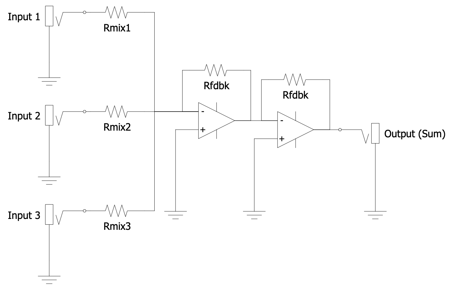
Example 10: Virtual Ground Active Mixer
This diagram was created in ConceptDraw DIAGRAM using a combination of libraries from the Analog Electronics Solution. An experienced user spent 10 minutes creating this sample.
This sample shows a virtual ground active additive mixer. It is an electronic device that combines two or more electronic or electrical signals into one or two output signals. The buffer amplifiers are intended to reduce crosstalk and distortion. Additive mixers are analog adders and add the values of two or more signals at some point. They use Kirchhoff's circuit laws to add the currents of signals together. As a result, they provide a composite signal containing the frequency components of each of the original signals. This is a continuous waveform. Additive mixers are used effectively in audio electronics for mixing voice, music, and audio signals. The simplest additive mixers only include resistors so that the signal sources do not interfere with each other. More complex options contain transistors, diodes, buffer amplifiers, arranged in a balanced or double balanced circuit. Made in the form of monolithic or hybrid integrated circuits, they are suitable for a wide range of frequency ranges.
Inside
What I Need to Get Started
Both ConceptDraw DIAGRAM drawing software and the Analogue Electronics solution can help creating the illustrations the technical documentation of an engineering projects you need. The Analogue Electronics solution can be found in the Industrial Engineering area of ConceptDraw STORE application that can be downloaded from this site. Make sure that both ConceptDraw DIAGRAM and ConceptDraw STORE applications are installed on your computer before you get started.
How to install
After ConceptDraw STORE and ConceptDraw DIAGRAM are downloaded and installed, you can install the Analogue Electronics solution from the ConceptDraw STORE.

Start Using
To make sure that you are doing it all right, use the pre-designed symbols from the stencil libraries from the solution to make your drawings look smart and professional. Also, the pre-made examples from this solution can be used as drafts so your own drawings can be based on them. Using the samples, you can always change their structures, colors and data.
