- Electric and Telecom Plans Free
- Fire and Emergency Plans Free
- Floor Plans Free
- Plant Layout Plans Free
- School and Training Plans Free
- Seating Plans Free
- Security and Access Plans Free
- Site Plans Free
- Sport Field Plans Free
- Business Process Diagrams Free
- Business Process Mapping Free
- Classic Business Process Modeling Free
- Cross-Functional Flowcharts Free
- Event-driven Process Chain Diagrams Free
- IDEF Business Process Diagrams Free
- Logistics Flow Charts Free
- Workflow Diagrams Free
- ConceptDraw Dashboard for Facebook Free
- Mind Map Exchange Free
- MindTweet Free
- Note Exchange Free
- Project Exchange Free
- Social Media Response Free
- Active Directory Diagrams Free
- AWS Architecture Diagrams Free
- Azure Architecture Free
- Cisco Network Diagrams Free
- Cisco Networking Free
- Cloud Computing Diagrams Free
- Computer Network Diagrams Free
- Google Cloud Platform Free
- Interactive Voice Response Diagrams Free
- Network Layout Floor Plans Free
- Network Security Diagrams Free
- Rack Diagrams Free
- Telecommunication Network Diagrams Free
- Vehicular Networking Free
- Wireless Networks Free
- Comparison Dashboard Free
- Composition Dashboard Free
- Correlation Dashboard Free
- Frequency Distribution Dashboard Free
- Meter Dashboard Free
- Spatial Dashboard Free
- Status Dashboard Free
- Time Series Dashboard Free
- Basic Circle-Spoke Diagrams Free
- Basic Circular Arrows Diagrams Free
- Basic Venn Diagrams Free
- Block Diagrams Free
- Concept Maps Free
- Family Tree Free
- Flowcharts Free
- Basic Area Charts Free
- Basic Bar Graphs Free
- Basic Divided Bar Diagrams Free
- Basic Histograms Free
- Basic Line Graphs Free
- Basic Picture Graphs Free
- Basic Pie Charts Free
- Basic Scatter Diagrams Free
- Aerospace and Transport Free
- Artwork Free
- Audio, Video, Media Free
- Business and Finance Free
- Computers and Communications Free
- Holiday Free
- Manufacturing and Maintenance Free
- Nature Free
- People Free
- Presentation Clipart Free
- Safety and Security Free
- Analog Electronics Free
- Audio and Video Connectors Free
- Basic Circuit Diagrams Free
- Chemical and Process Engineering Free
- Digital Electronics Free
- Electrical Engineering Free
- Electron Tube Circuits Free
- Electronic Block Diagrams Free
- Fault Tree Analysis Diagrams Free
- GHS Hazard Pictograms Free
- Home Automation and Wiring Free
- Mechanical Engineering Free
- One-line Diagrams Free
- Power Сircuits Free
- Specification and Description Language (SDL) Free
- Telecom and AV Circuits Free
- Transport Hazard Pictograms Free
- Data-driven Infographics Free
- Pictorial Infographics Free
- Spatial Infographics Free
- Typography Infographics Free
- Calendars Free
- Decision Making Free
- Enterprise Architecture Diagrams Free
- Fishbone Diagrams Free
- Organizational Charts Free
- Plan-Do-Check-Act (PDCA) Free
- Seven Management and Planning Tools Free
- SWOT and TOWS Matrix Diagrams Free
- Timeline Diagrams Free
- Australia Map Free
- Continent Maps Free
- Directional Maps Free
- Germany Map Free
- Metro Map Free
- UK Map Free
- USA Maps Free
- Customer Journey Mapping Free
- Marketing Diagrams Free
- Matrices Free
- Pyramid Diagrams Free
- Sales Dashboard Free
- Sales Flowcharts Free
- Target and Circular Diagrams Free
- Cash Flow Reports Free
- Current Activities Reports Free
- Custom Excel Report Free
- Knowledge Reports Free
- MINDMAP Reports Free
- Overview Reports Free
- PM Agile Free
- PM Dashboards Free
- PM Docs Free
- PM Easy Free
- PM Meetings Free
- PM Planning Free
- PM Presentations Free
- PM Response Free
- Resource Usage Reports Free
- Visual Reports Free
- House of Quality Free
- Quality Mind Map Free
- Total Quality Management TQM Diagrams Free
- Value Stream Mapping Free
- Astronomy Free
- Biology Free
- Chemistry Free
- Language Learning Free
- Mathematics Free
- Physics Free
- Piano Sheet Music Free
- Android User Interface Free
- Class Hierarchy Tree Free
- Data Flow Diagrams (DFD) Free
- DOM Tree Free
- Entity-Relationship Diagram (ERD) Free
- EXPRESS-G data Modeling Diagram Free
- IDEF0 Diagrams Free
- iPhone User Interface Free
- Jackson Structured Programming (JSP) Diagrams Free
- macOS User Interface Free
- Object-Role Modeling (ORM) Diagrams Free
- Rapid UML Free
- SYSML Free
- Website Wireframe Free
- Windows 10 User Interface Free
Digital Electronics
Digital electronics or digital circuits is a field of electronics studying the digital signals and engineering devices producing them. It uses digital signals to perform varied tasks and meet different requirements. Digital electronic circuits are usually made from large assemblies of logic gates implemented using diodes, transistors, and relays. The logic gates use Boolean functions. There are AND, OR, NOT, NOR, NAND, XOR, and XNOR gates that perform logical operations, often they are packaged in integrated circuits. AND, OR, NOT are basic gates, while NAND and OR are universal gates. Usually, a combination of different logic gates is used.
Digital circuits use relays, vacuum tubes, CMOS logic, transistor-transistor logic (TTL), emitter-coupled logic, etc. The input signal has a binary format and is represented by 0 or 1. The output obtained by processing digital data has a precise value. Typically, a logical truth table and timing diagram are used to demonstrate the mathematical representation of the characteristics of digital signals passing through a digital circuit. They show input and output of digital data. The logical truth table consists of 3 columns: clock column, input column and output column. The behavior of a digital signal is presented in a time domain format. For example, for a NOT gate, when the clock signal is high, the input is low and the output is high, and accordingly, when the input is high, the output is low.
As a rule, first, a logic diagram is constructed and then it is transformed into a working electrical circuit. Each electrical component of the circuit is shown by a special symbol in the diagram. The direction of connection lines may go everywhere regardless of the flow of the signal. Moreover, the lines may intersect. In an effort to reduce cost, reduce potential errors, and avoid logical redundancy, engineers seek to reduce circuit complexity. Representing a digital circuit as a set of logic elements is a classic way in electronics. Another way is to build a system of electronic switches or transistors and represent it as a truth table.
There are used synchronous and asynchronous systems. Synchronous systems change their states when clock signals change states. Asynchronous systems change states when inputs are changed, their speed is not limited by an arbitrary clock and they run at the maximum speed of the corresponding logic gates. Most digital logic is synchronous, however, the combination with asynchronous parts makes the circuit faster.
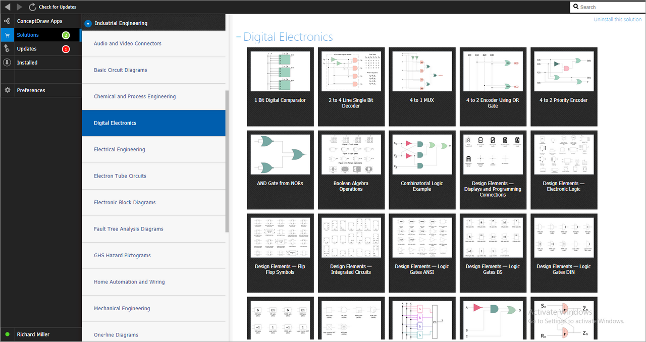
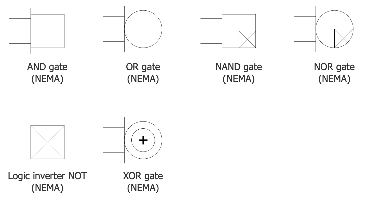
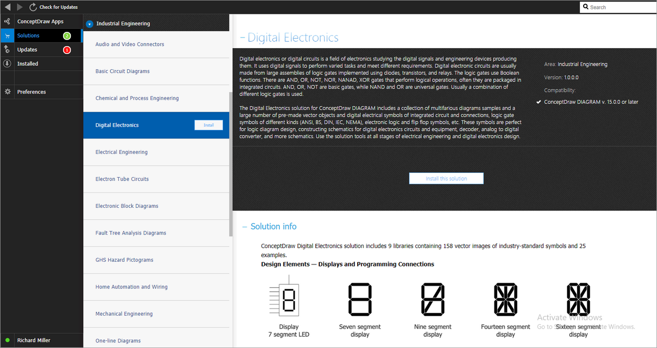
The Digital Electronics solution for ConceptDraw DIAGRAM includes a collection of multifarious diagrams samples and a large number of pre-made vector objects and digital electrical symbols of integrated circuit and connections, logic gate symbols of different kinds (ANSI, BS, DIN, IEC, NEMA), electronic logic and flip flop symbols, etc. These symbols are perfect for logic diagram design, constructing schematics for digital electronics circuits and equipment, decoder, analog to digital converter, and more schematics. Use the solution tools at all stages of electrical engineering and digital electronics design.
-
What I need to get started -
Solution Requirements - This solution requires the following products to be installed:
ConceptDraw DIAGRAM v18 - This solution requires the following products to be installed:
-
Helpdesk
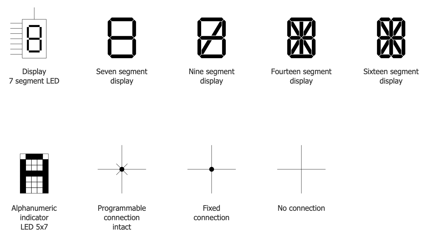
Design Elements — Displays and Programming Connections
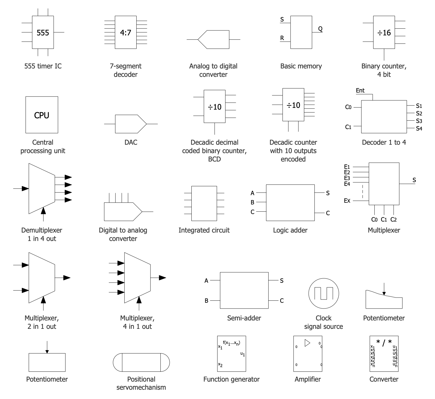
Design Elements — Electronic Logic
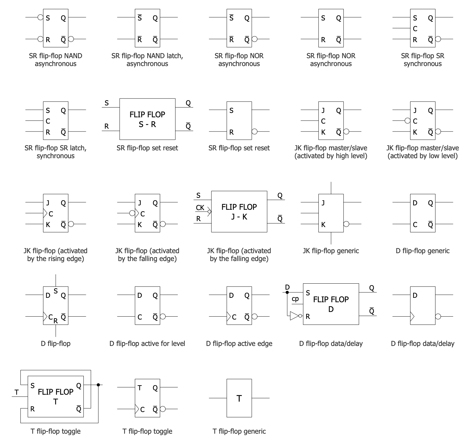
Design Elements — Flip Flop Symbols
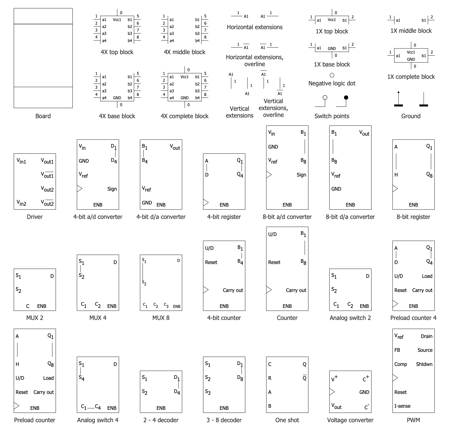
Design Elements — Integrated Circuits
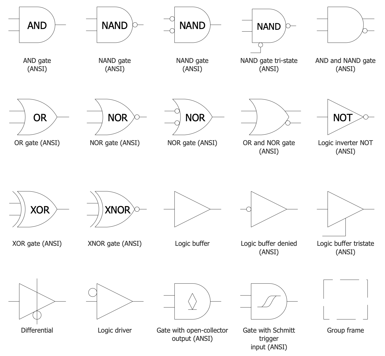
Design Elements — Logic Gates ANSI
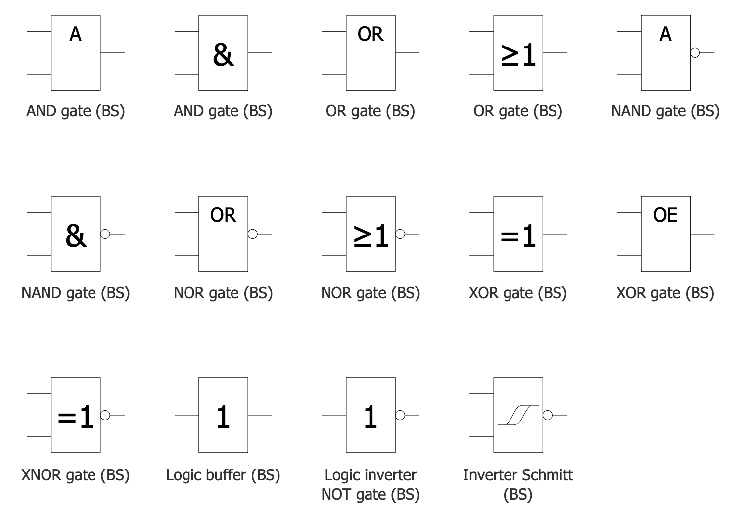
Design Elements — Logic Gates BS
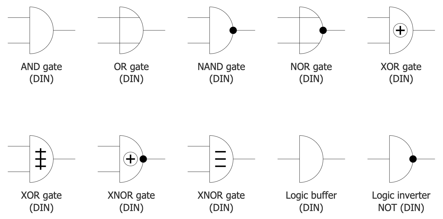
Design Elements — Logic Gates DIN
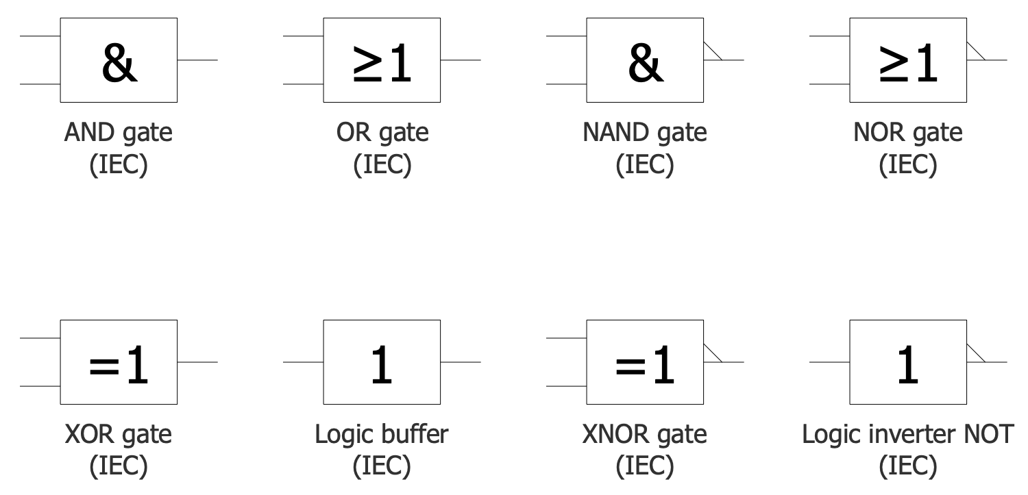
Design Elements — Logic Gates IEC
Design Elements — Logic Gates NEMA
Related News:
Examples
There are a few samples that you see on this page which were created in the ConceptDraw DIAGRAM application by using the Digital Electronics solution. Some of the solution's capabilities as well as the professional results which you can achieve are all demonstrated here on this page.
All source documents are vector graphic documents which are always available for modifying, reviewing and/or converting to many different formats, such as MS PowerPoint, PDF file, MS Visio, and many other graphic ones from the ConceptDraw Solution Park or ConceptDraw STORE. The Digital Electronics solutions are available to all ConceptDraw DIAGRAM users to install and use it for working in diagramming and drawing.
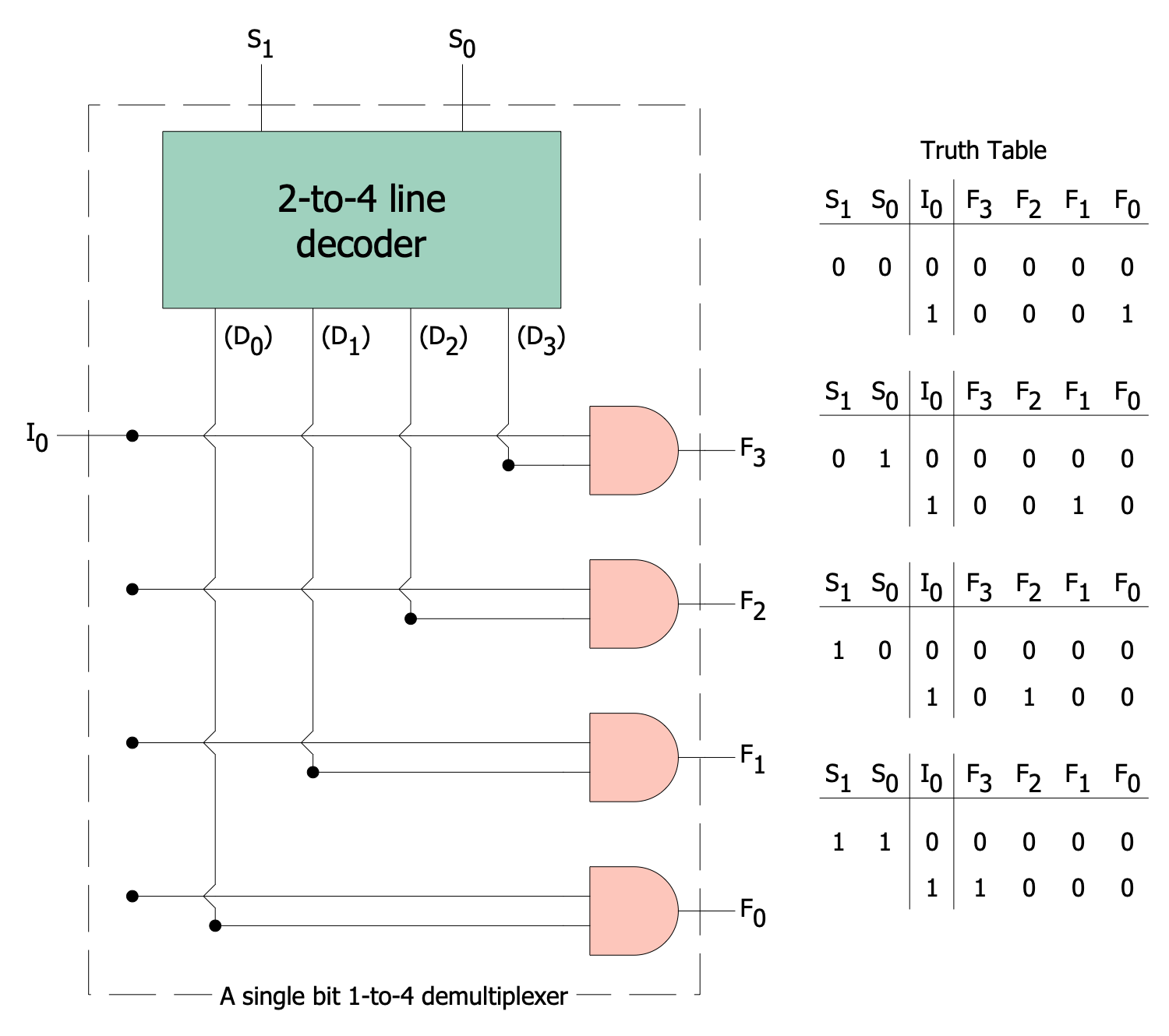
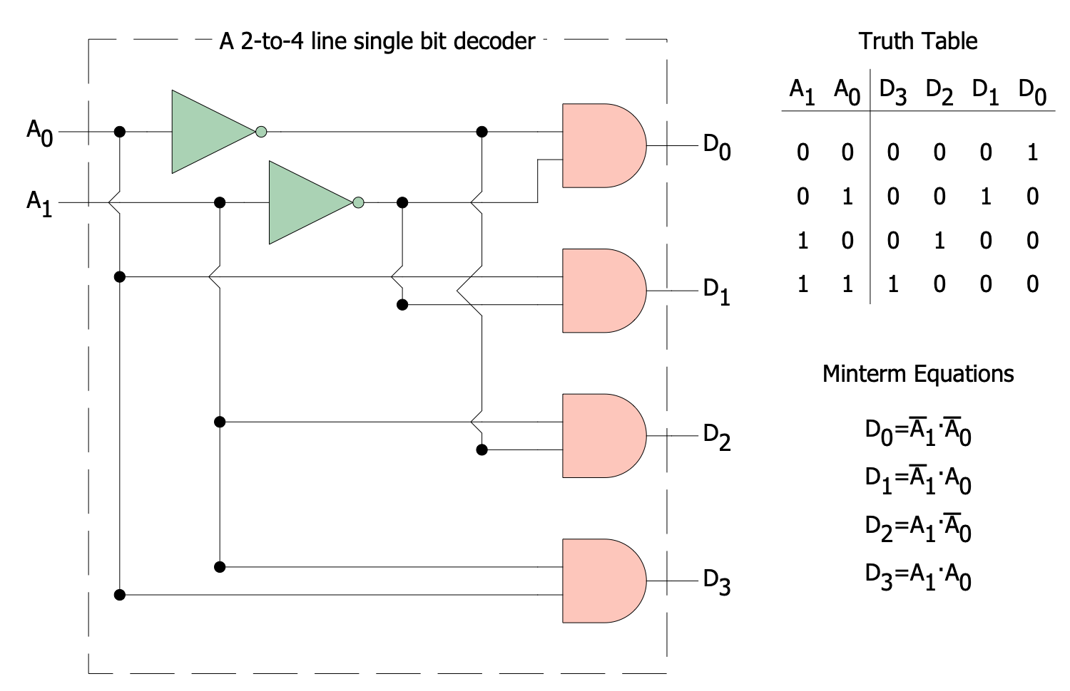
Example 1: 2 to 4 Line Single Bit Decoder
This diagram was created in ConceptDraw DIAGRAM using a combination of libraries from the Digital Electronics Solution. An experienced user spent 10 minutes creating this sample.
This digital electronic circuit diagram example shows a 2-to-4 line single bit decoder with a truth table and minterm equations. A binary decoder is an electronic circuit with combinational logic. It includes multiple coded inputs and multiple outputs. A primary purpose is to convert binary information from the n input signals to 2n unique output signals. When a decoder has less than 2n outputs, at least one output will be the same for different input values. As a rule, the data inputs of the binary decoders are integers. As for the implementation, a binary decoder is designed in one of two ways: as a stand-alone integrated circuit (IC) or as part of a complex IC. A binary decoder has a wide variety of applications and is mainly applied in the form of the standardized IC. Common applications include data multiplexing, data demultiplexing, instruction decoding, memory address decoding, and more.
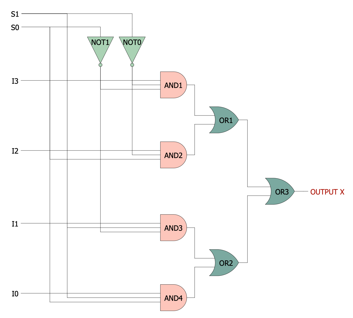
Example 2: 4 to 1 MUX
This diagram was created in ConceptDraw DIAGRAM using a combination of libraries from the Digital Electronics Solution. An experienced user spent 10 minutes creating this sample.
This digital electronic logic diagram example shows a 4 to 1 multiplexer (MUX) using 4 inputs AND, 3 inputs OR, 2 NOT gates. The inputs are shown as I0, I1, I2, I3; the output X depends on the selector lines S0 and S1. A multiplexer selects a single input signal among several analog or digital signals and sends it to a single output line. That is why it is also called data selector. This selection is made using selector lines, which are a separate set of digital inputs. A multiplexer with 2n inputs has n selector lines. In this regard, an electronic multiplexer is often considered as a multiple-input rotary switch or single-output switch. Digital multiplexers are constructed from high-speed logic gates. Analog multiplexers use transistors, MOSFET’s or relays. In this case, different inputs can share the same device or resource. Often, multiplexers are used to implement Boolean functions with multiple variables.
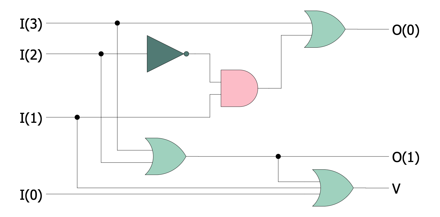
Example 3: 4 to 2 Priority Encoder
This diagram was created in ConceptDraw DIAGRAM using a combination of libraries from the Digital Electronics Solution. An experienced user spent 10 minutes creating this sample.
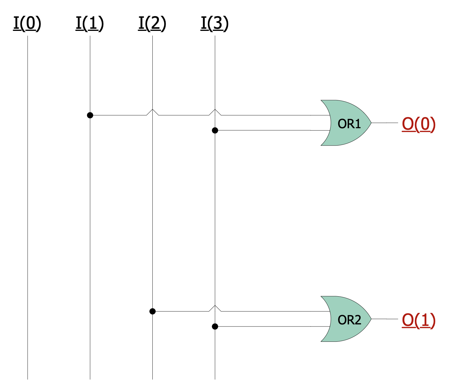
This digital electronics diagram example shows a single bit 4 to 2 priority encoder. It is a circuit or algorithm used to compress multiple binary inputs into outputs, at this the number of outputs is smaller than inputs. It allows handling the multifarious input configurations. The output has a binary representation, starts from zero, and presents the index of the most significant of the activated lines. Often priority decoders are used to manage interrupt requests. Of two or more inputs, the one with the highest priority will take precedence. The priority decoder will act on this highest priority input. The inputs I0, I1, I2, I3 are shown in a diagram. Some of them will have an irrelevant value — their input value will be replaced by the value of the highest-priority input. The output V reveals if the input is valid. Sometimes, the priority encoders are connected in arrays and form larger encoders.
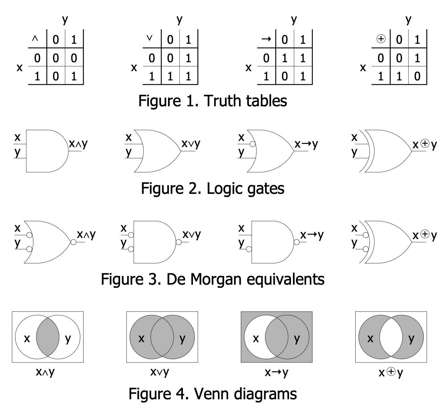
Example 4: Boolean Algebra Operations
This diagram was created in ConceptDraw DIAGRAM using a combination of libraries from the Digital Electronics Solution. An experienced user spent 10 minutes creating this sample.
This digital electronic diagram example shows multiple representations of Boolean algebra operations. You can observe four figures showing the principles of use of the truth tables, logic gates, de Morgan equivalents, and Venn diagrams. Boolean algebra or logical algebra is a part of mathematics focused on operating with binary variables taking one of two values True (1) or False (0). Boolean Algebra is based on logic and has its own set of rules for making Boolean expressions. The main operations include conjunction (AND), disjunction (OR), exclusive OR (XOR), and negation (NOT). Boolean AND and OR are similar to binary multiplication and addition respectively. The application of Boolean algebra is widespread in the process of developing different kinds of digital electronics. All logic operations are presented as expressions or equations using Boolean algebra. Boolean equations are used to analyze digital gates and electronic circuits. They give an overview of an electronic circuit design and behavior in a simple and clear form.
Example 5: Flip Flop Logic Circuit
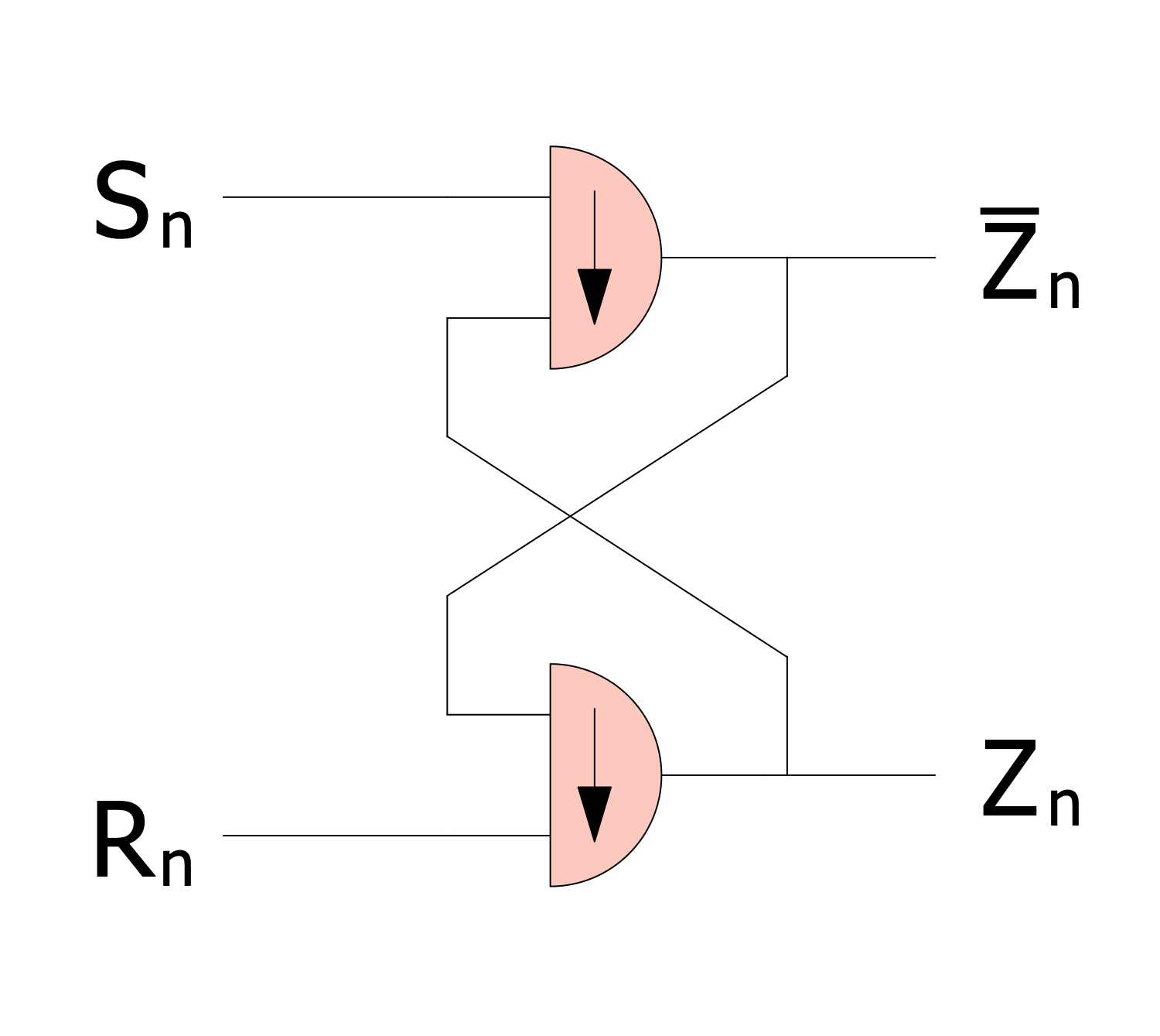
This diagram was created in ConceptDraw DIAGRAM using a combination of libraries from the Digital Electronics Solution. An experienced user spent 10 minutes creating this sample.
This digital electronic diagram example shows a flip-flop logic circuit. Flip-flops are ones of the basic building blocks of digital electronics systems including computers, communications, and much more. A flip-flop is a circuit that stores state information as a single bit. Flip-flops are the elements of sequential logic in electronics and have two stable states (0 or 1). Special settings allow you to configure the system to change its state depending on the signal applied to one of the control inputs. As for the outputs, the circuit has one or two. There are used both level-triggered and edge-triggered flip-flops. They are asynchronous and synchronous, respectively. The former are also transparent — any changes in the input signal cause immediate changes in the output signal. The represented trigger has the SR ("set-reset") type that influences its behavior. It consists of a pair of cross-coupled logic gates. The outputs marked Zn are in a constant state.
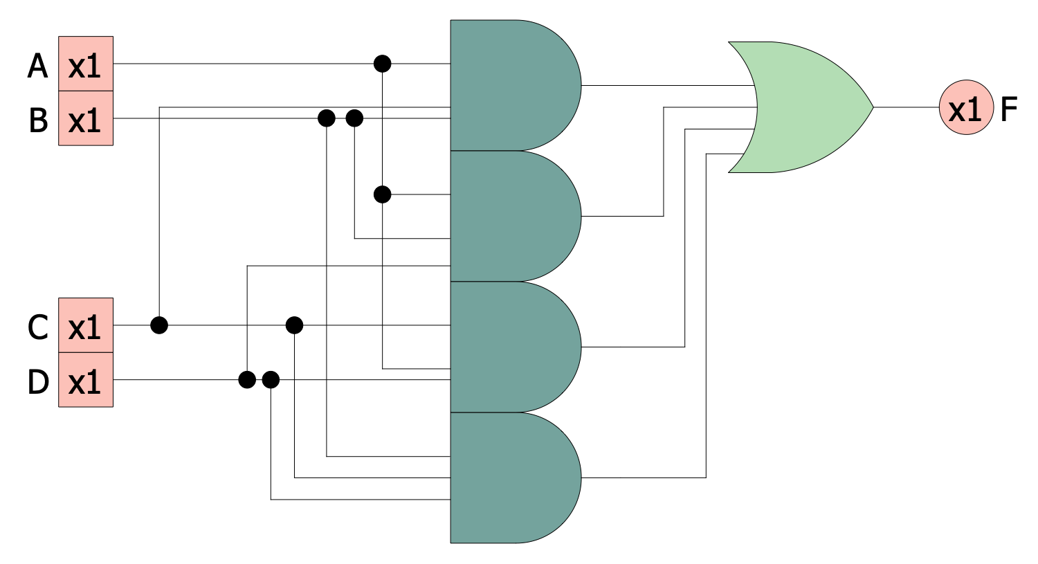
Example 6: Four Bit Majority Circuit
This diagram was created in ConceptDraw DIAGRAM using a combination of libraries from the Digital Electronics Solution. An experienced user spent 10 minutes creating this sample.
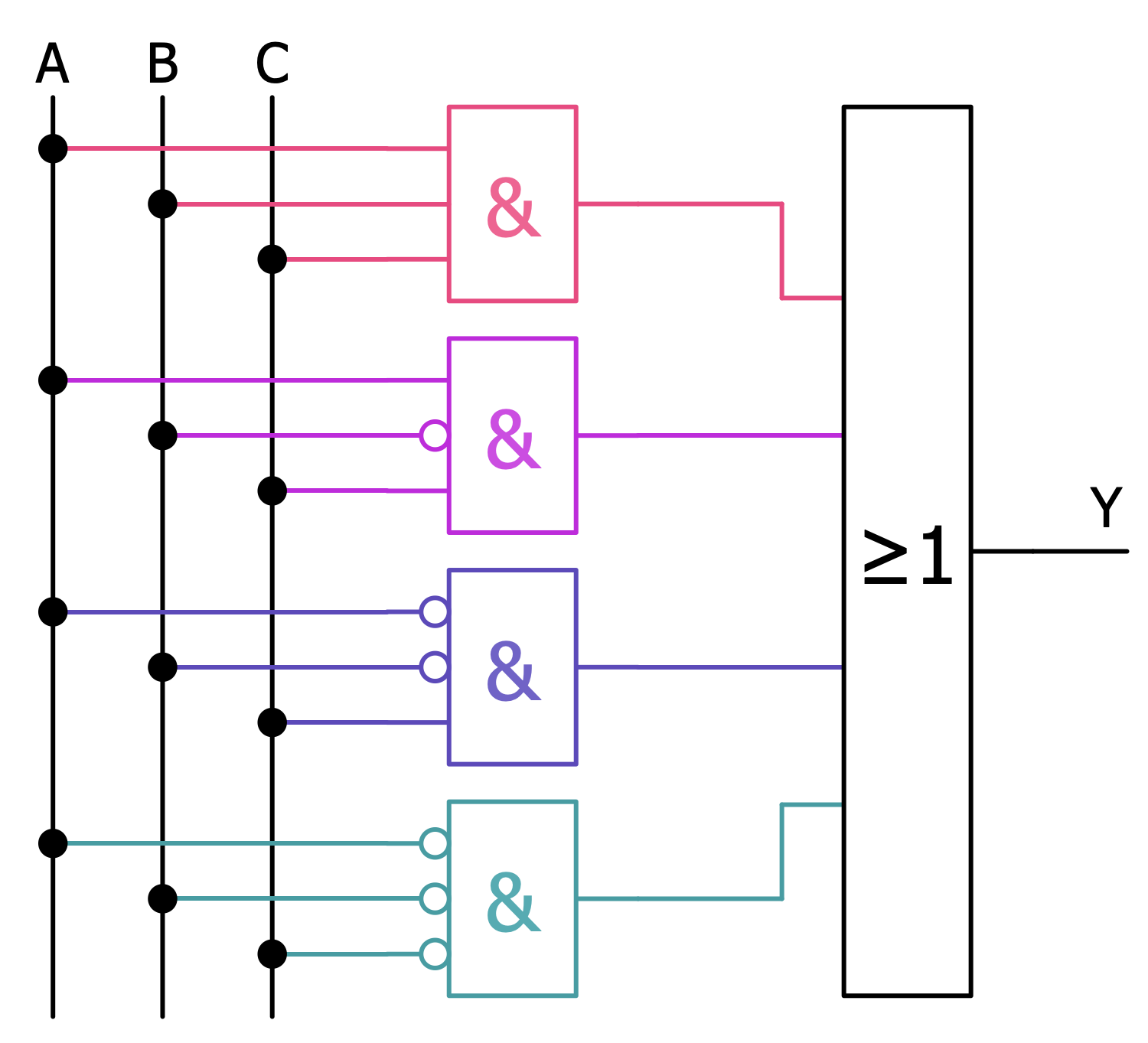
This digital electronic diagram example shows a 4-bit majority circuit. A majority function is a Boolean function and takes the value of the majority of the inputs. In this way, it takes true value when half or more arguments are true and false otherwise. A majority gate is a logical gate used in Boolean circuits. Similarly, it returns true only if half or more than half of the inputs are true. Thereby, the 4-input majority gate has 0 output only when two or more of its inputs have 0 value, and similarly in the case of value 1. The use of the majority function provides majority logic decoding and allows the implementation of errors correction. 4-bit majority circuits have a wide application but there are systems with different quantities like systems with 3-bit majority circuits. ConceptDraw DIAGRAM with Digital Electronics solution makes it easy and fast to design most circuits for different numbers of bits using pre-programmed digital and electrical symbols. Each schematic will be precise and easy to understand.
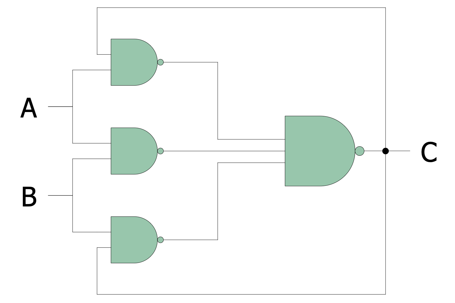
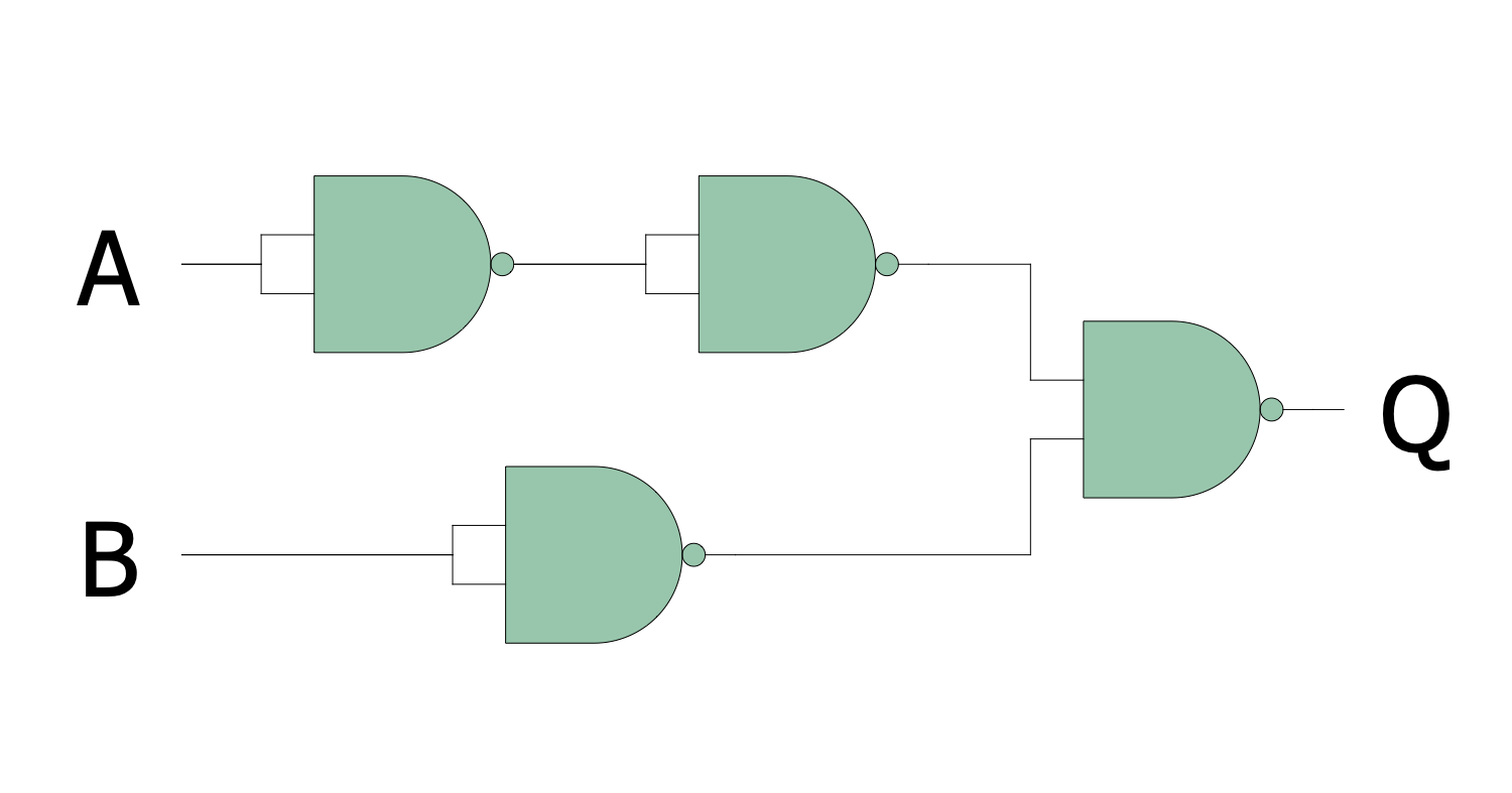
Example 7: IMPLY Gate from NANDs
This diagram was created in ConceptDraw DIAGRAM using a combination of libraries from the Digital Electronics Solution. An experienced user spent 10 minutes creating this sample.
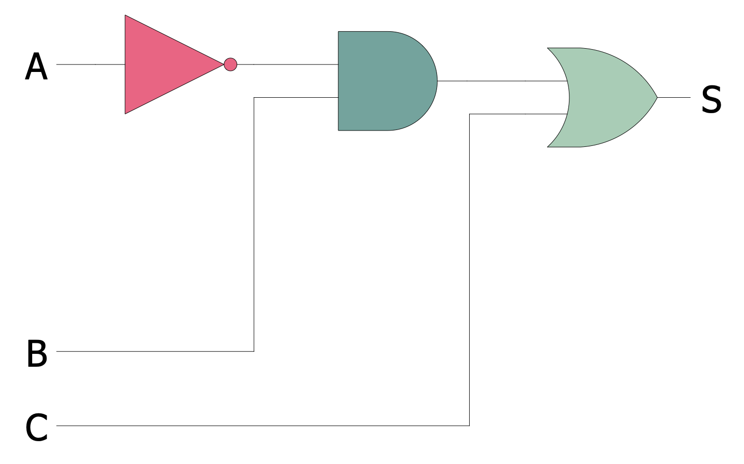
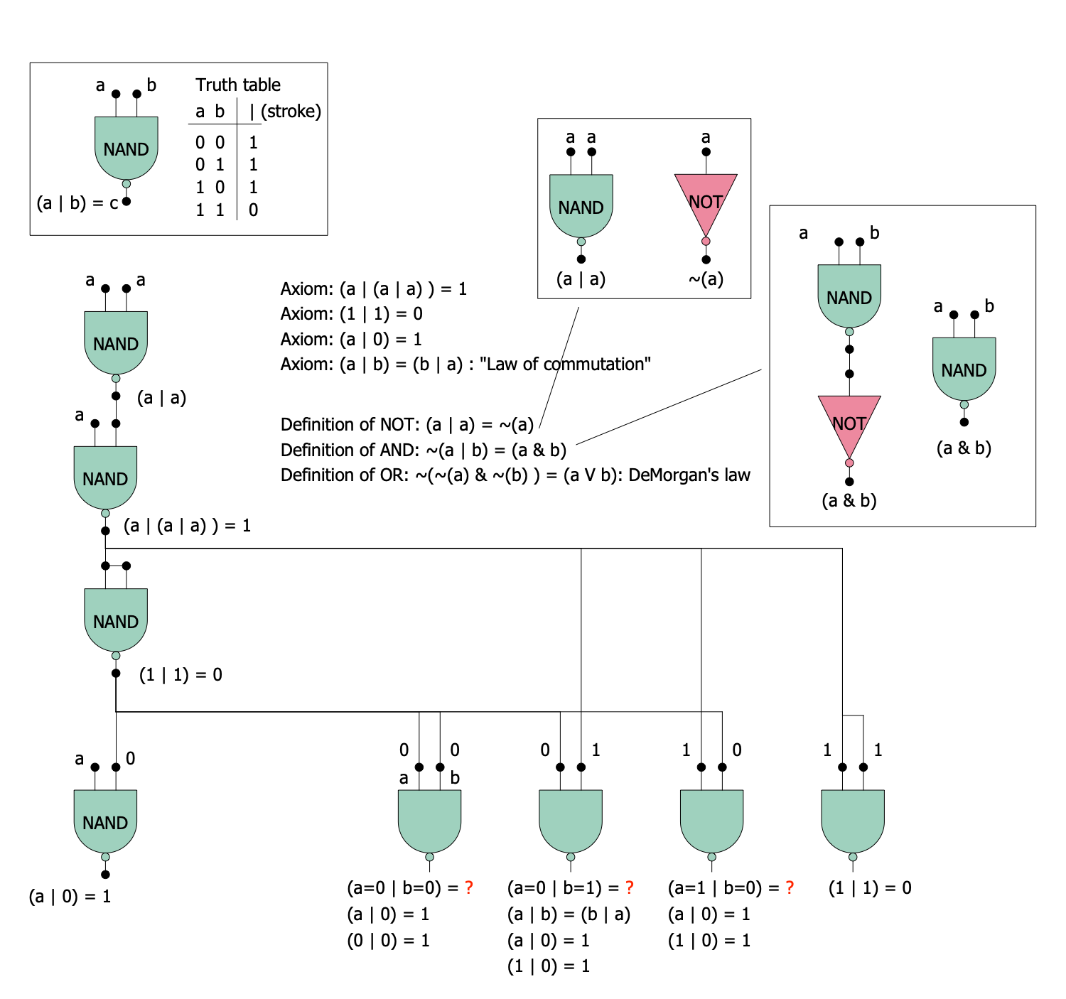
This digital electronic circuit diagram example shows an IMPLY gate made of NAND gates. IMPLY gate is a digital logic gate, that implements a logical conditional between inputs. It produces a result equal to the value of the second input when the first input is true and true otherwise. In turn, NOT-AND (NAND) gate is also a logic gate, it produces a false output only if all its inputs are true and vice versa. If any input is false or true, the output takes the true or false value respectively. As a result, its output supplements the output of the AND gate. Typically, NAND gates include two or more inputs and are available as integrated circuits. NAND gates are constructed using transistors and junction diodes. In addition, they provide functional completeness because any boolean function can be implemented using a combination of NAND gates. This is an important advantage used by most digital electronic systems with NAND gates.
Example 8: Logic Circuit Example
This diagram was created in ConceptDraw DIAGRAM using a combination of libraries from the Digital Electronics Solution. An experienced user spent 10 minutes creating this sample.
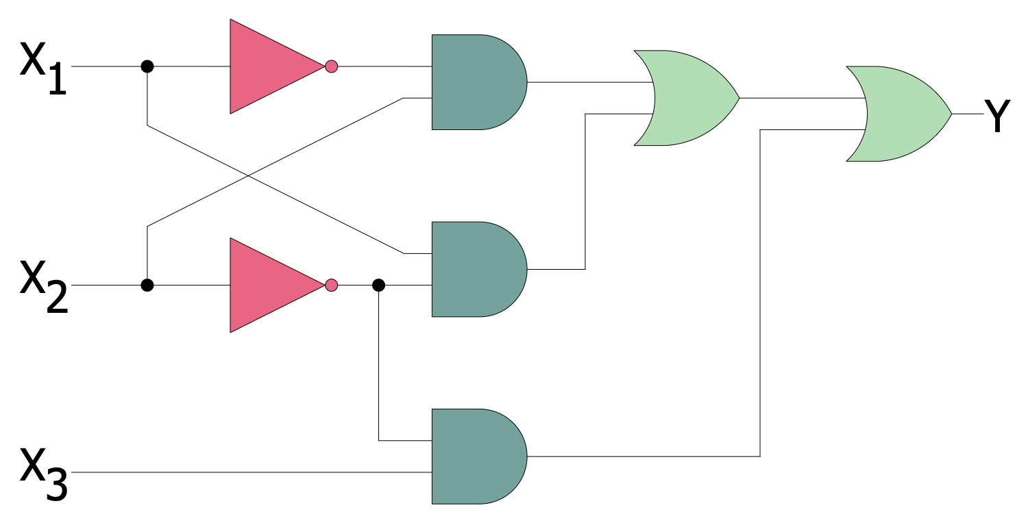
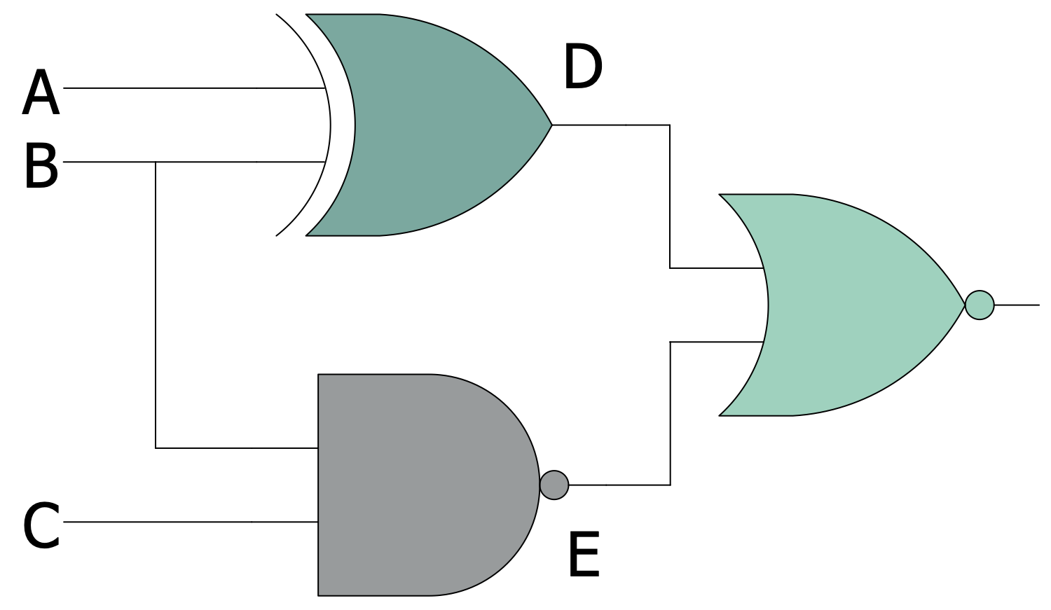
This digital electronic diagram shows an example of a logic circuit containing XOR, NAND, and NOR gates. They are used to construct both simple and complicated logic circuits. The different types of gates are connected to produce complicated switching circuits. A logic gate is an idealized model of a physical electronic device or computing device. It has one or more binary inputs, produces a single binary output, and uses logical operations or Boolean functions. As a rule, logic gates are constructed using diodes or transistors and act as electronic switches. It is an example of the combinational logic circuit and the output depends on the inputs. Moreover, any changes in input signals cause changes in the output. The vacuum tubes, pneumatic logic, optics, fluidic logic, electromagnetic relays, multiplexers, registers, microprocessors, and more elements are also used to build the logic gates. Today most gates are constructed of the metal–oxide–semiconductor field-effect transistors (MOSFETs). Here, the logic gates are shown using the predesigned logic gate symbols from the solution libraries.
Example 9: MUX from 3 State Buffers
This diagram was created in ConceptDraw DIAGRAM using a combination of libraries from the Digital Electronics Solution. An experienced user spent 10 minutes creating this sample.
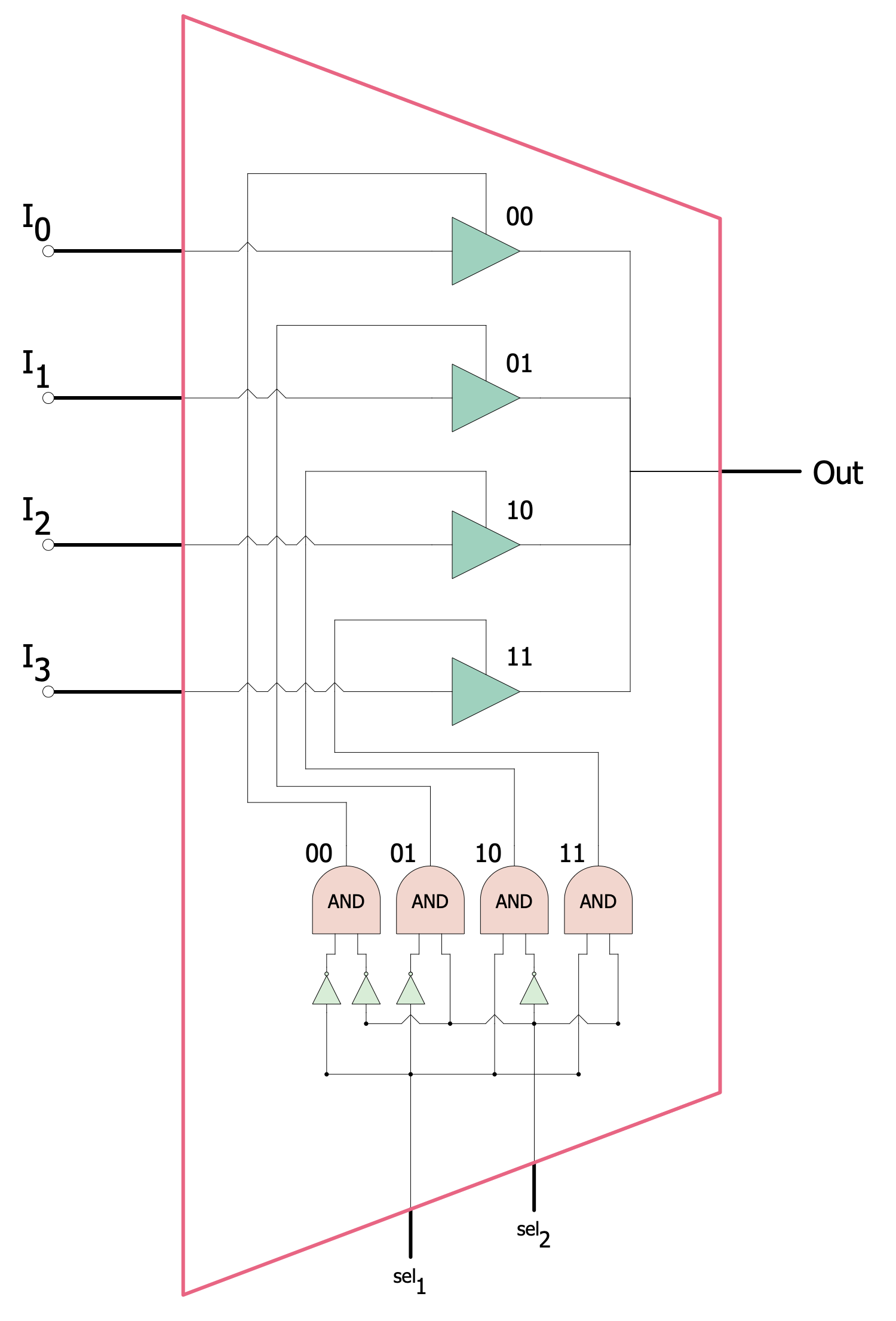
This diagram example shows a multiplexer (MUX) or a data selector realized from 3-state buffers and AND gates. It is an electronic device, which runs selection from analog or digital input signals. MUX includes several signal inputs, one or more control inputs, and one output. The signal transmission from one of several inputs to one output is the major function of a multiplexer. The selected input is forwarded to a single output line as a set of digital inputs (select lines). The 2n inputs multiplexer has n select lines. In this diagram, Sel1 and Sel2 are the control inputs. At this, Sel1 is more significant and Sel2 is less significant. The inputs are indicated by the decimal values at which the input is let through. The labels 00, 01, 10, and 11 indicate the turn-on code. A multiplexer makes possible the use of one device or resource for several input signals. Also, the multiplexers are used to implement Boolean functions of multiple variables.
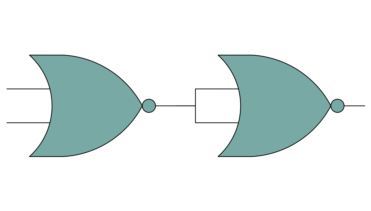
Example 10: NAND Gate from NORs
This diagram was created in ConceptDraw DIAGRAM using a combination of libraries from the Digital Electronics Solution. An experienced user spent 10 minutes creating this sample.
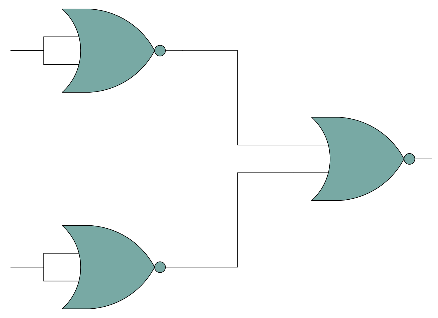
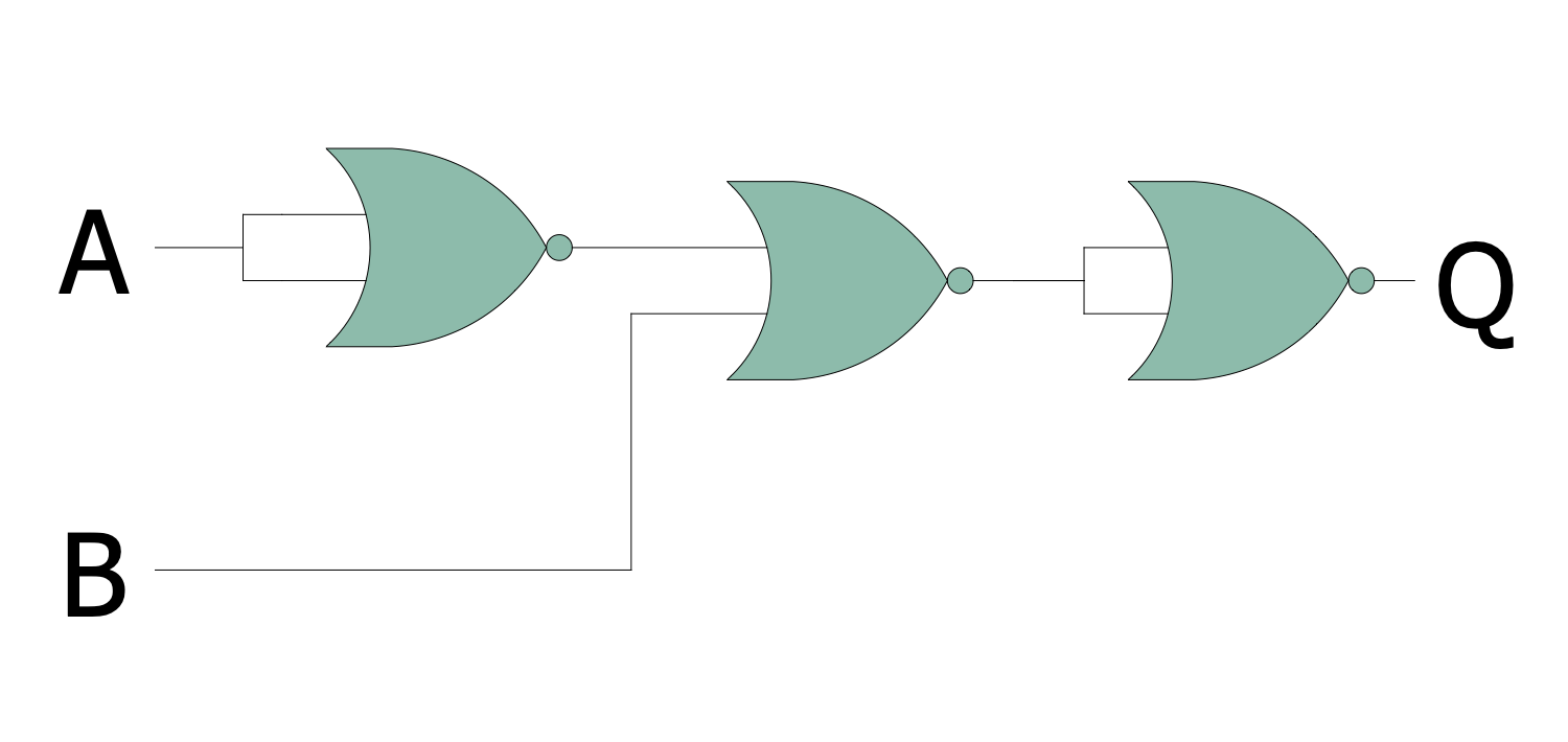
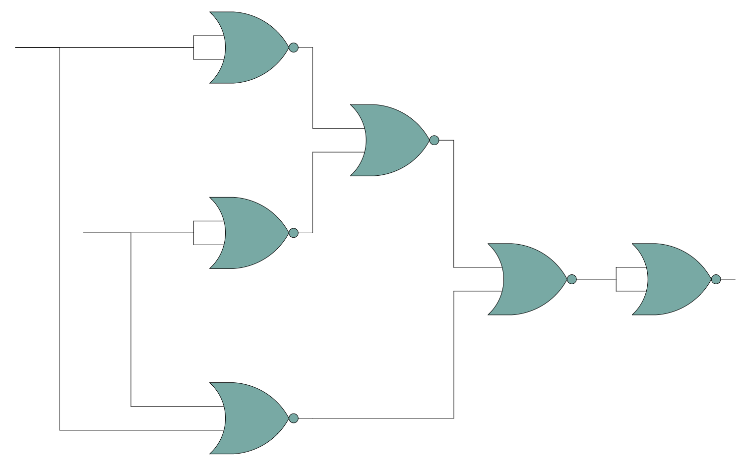
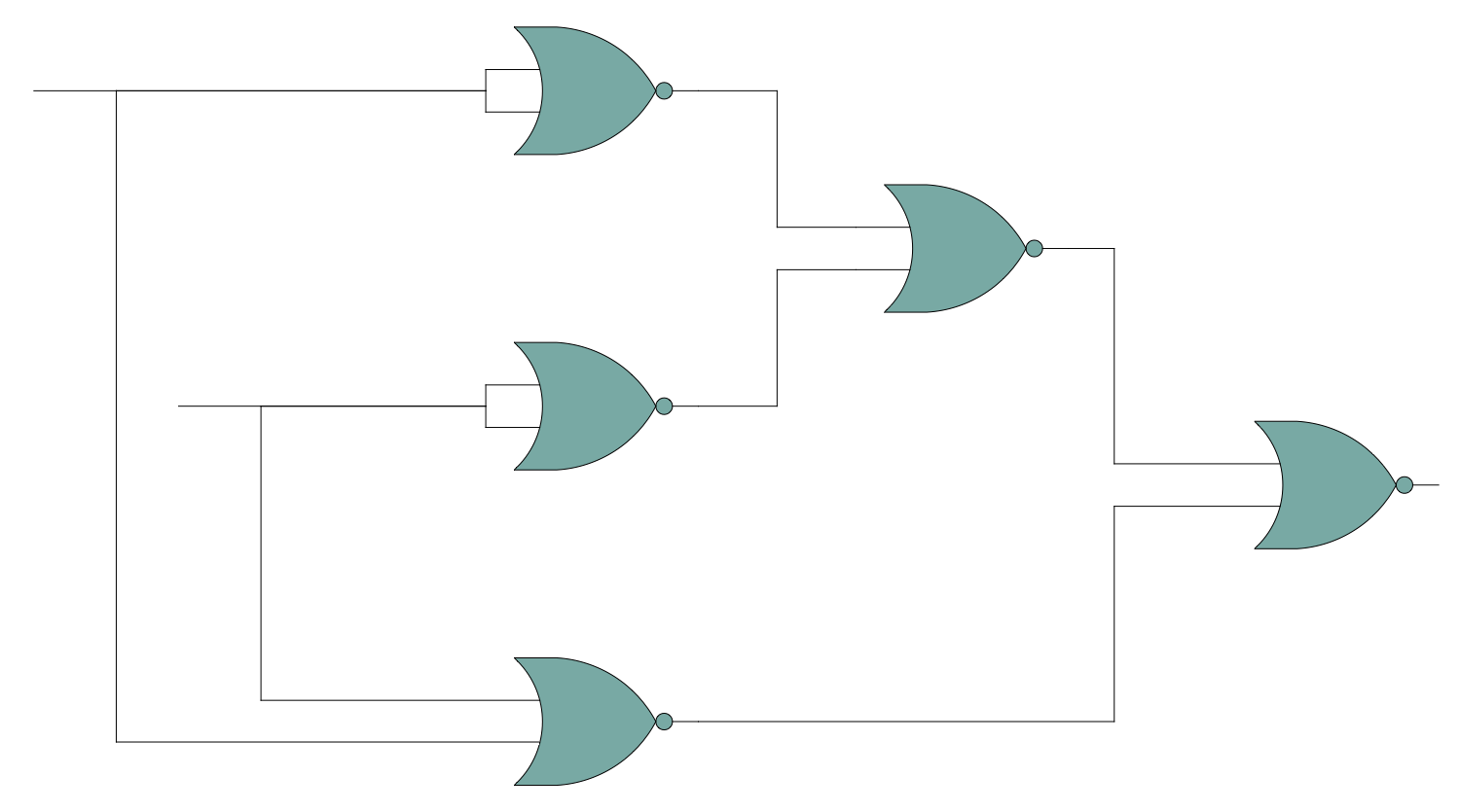
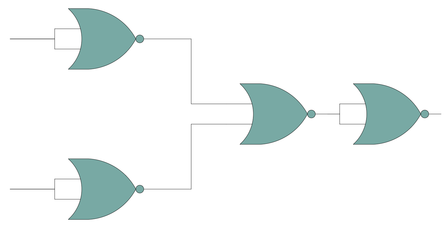
NAND gate is constructed using transistors and junction diodes and is an integrated circuit in transistor-transistor logic. NAND gate has two or more inputs and produces the output complementing to the AND gate. The output is false only when all inputs are true. If any input is false, an output is true. NOR gate is a digital logic gate, it implements logical NOR and is the negation of the OR operator. The output result of the NAND gate is true if both the inputs to the gate are false. If one or both inputs are true, the output is false. In general, NAND and NOR gates are functionally completed. That's why any Boolean function can be implemented by using a combination of NAND gates. ConceptDraw's Digital Electronics solution is perfect for easy designing any kind of digital electronic circuit diagrams, analog to digital converter schematics, and more charts.
Inside
What I Need to Get Started
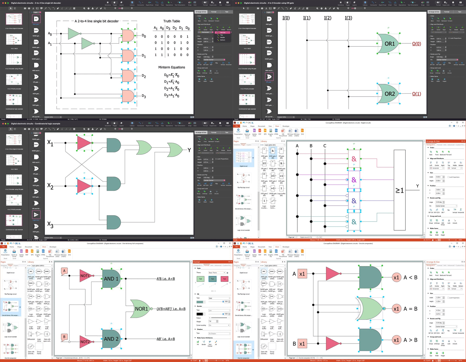
Both ConceptDraw DIAGRAM diagramming and drawing software and the Digital Electronics solution can help creating the illustrations the technical documentation of an engineering projects you need. The Digital Electronics solution can be found in the Industrial Engineering area of ConceptDraw STORE application that can be downloaded from this site. Make sure that both ConceptDraw DIAGRAM and ConceptDraw STORE applications are installed on your computer before you get started.
How to install
After ConceptDraw STORE and ConceptDraw DIAGRAM are downloaded and installed, you can install the Digital Electronics solution from the ConceptDraw STORE.
Start Using
To make sure that you are doing it all right, use the pre-designed symbols from the stencil libraries from the solution to make your drawings look smart and professional. Also, the pre-made examples from this solution can be used as drafts so your own drawings can be based on them. Using the samples, you can always change their structures, colors and data.
